Electronics Laboratory
The hardware backbone of A&D Lab — a fully equipped ESD-safe zone combining diagnostics, BGA rework, and environmental testing. We bring even the most complex electronic and opto-mechanical assemblies back to life.

Repair Technologies
A&D Serwis has been operating continuously since 1996. From the outset, we have specialized in the repair of advanced electronics, including high-integration circuits, multilayer laminates, and surface-mount technologies.
We followed and implemented the evolution of SMD, QFP, and BGA technologies in practice from the moment they became widespread in professional electronics. The experience gained working with multilayer boards and high-integration components today forms the foundation of our industrial equipment repair expertise.
Our early years were centered on repairing advanced computer electronics, which even then made use of multilayer laminates, SMD, QFP, and BGA packages. That experience became the foundation of the competencies we now apply to industrial electronics.
Modern industrial equipment such as:
- industrial computers
- operator panels
- frequency inverters
- industrial power supplies and UPS units
- PLC controllers
- IGBT power modules
contains circuitry with a level of integration comparable to modern computer systems. The difference lies in operating conditions, current loads, and the industrial environment. Our technical facility was built specifically for the diagnostics and repair of this class of electronics.
Thermal Imaging Diagnostics
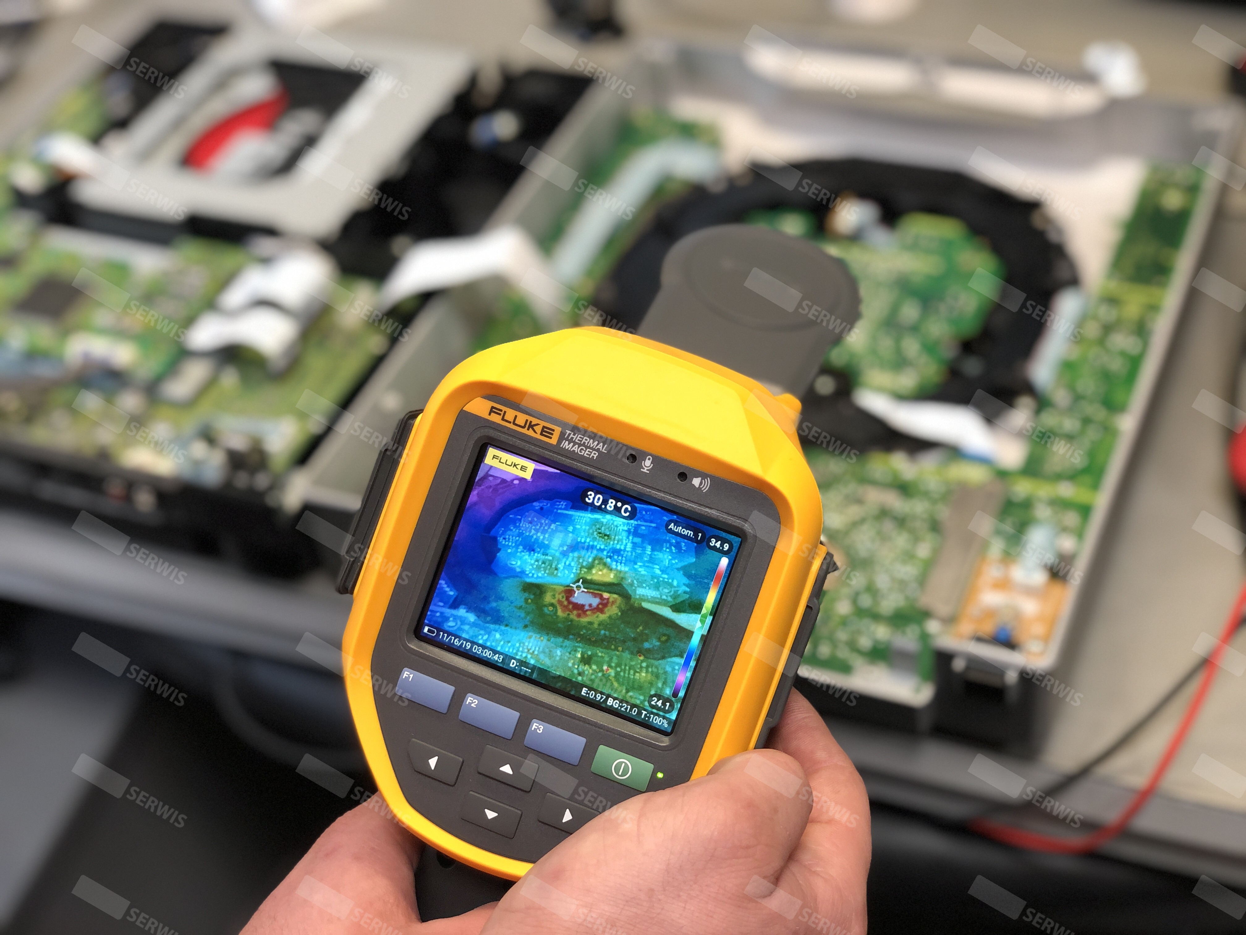
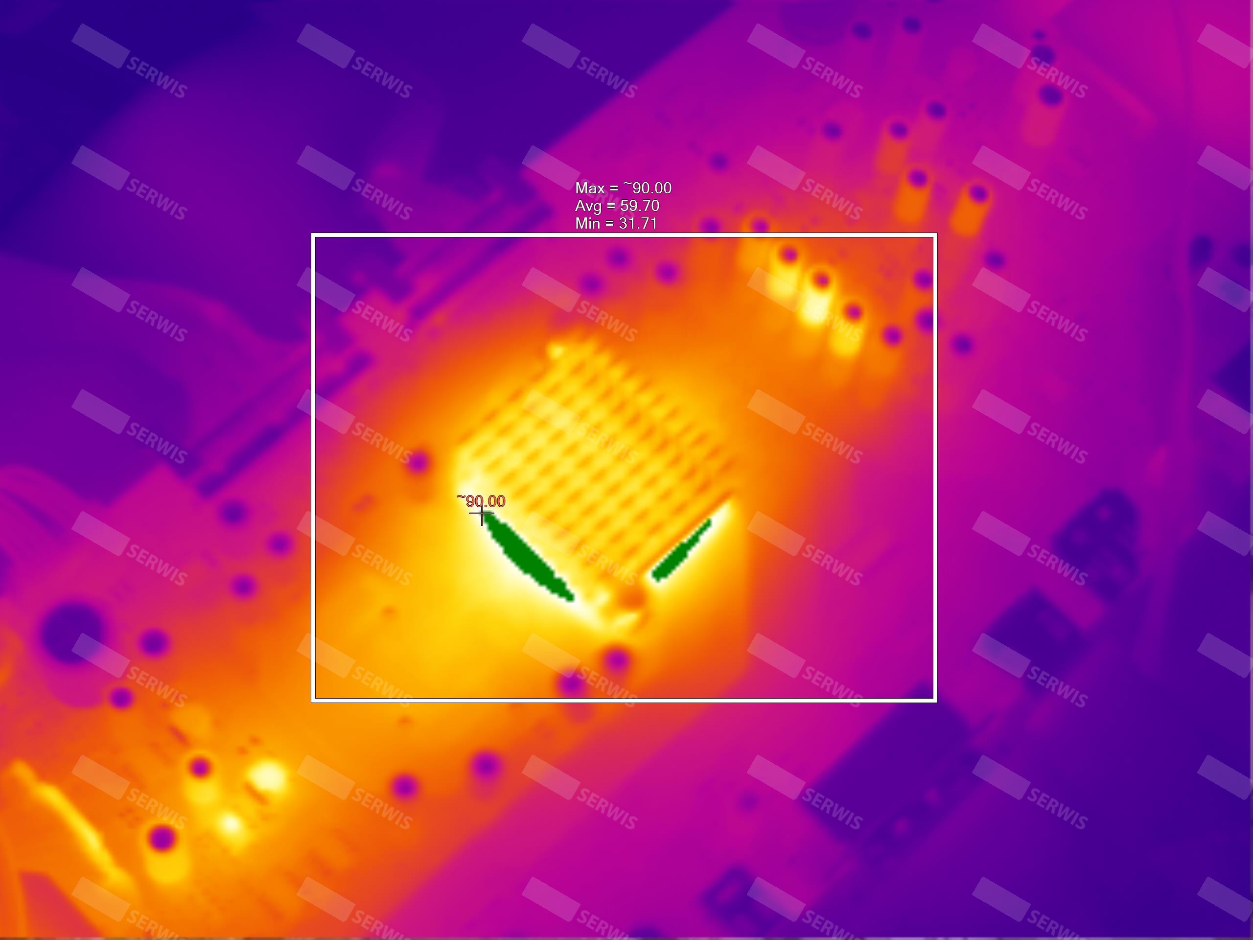
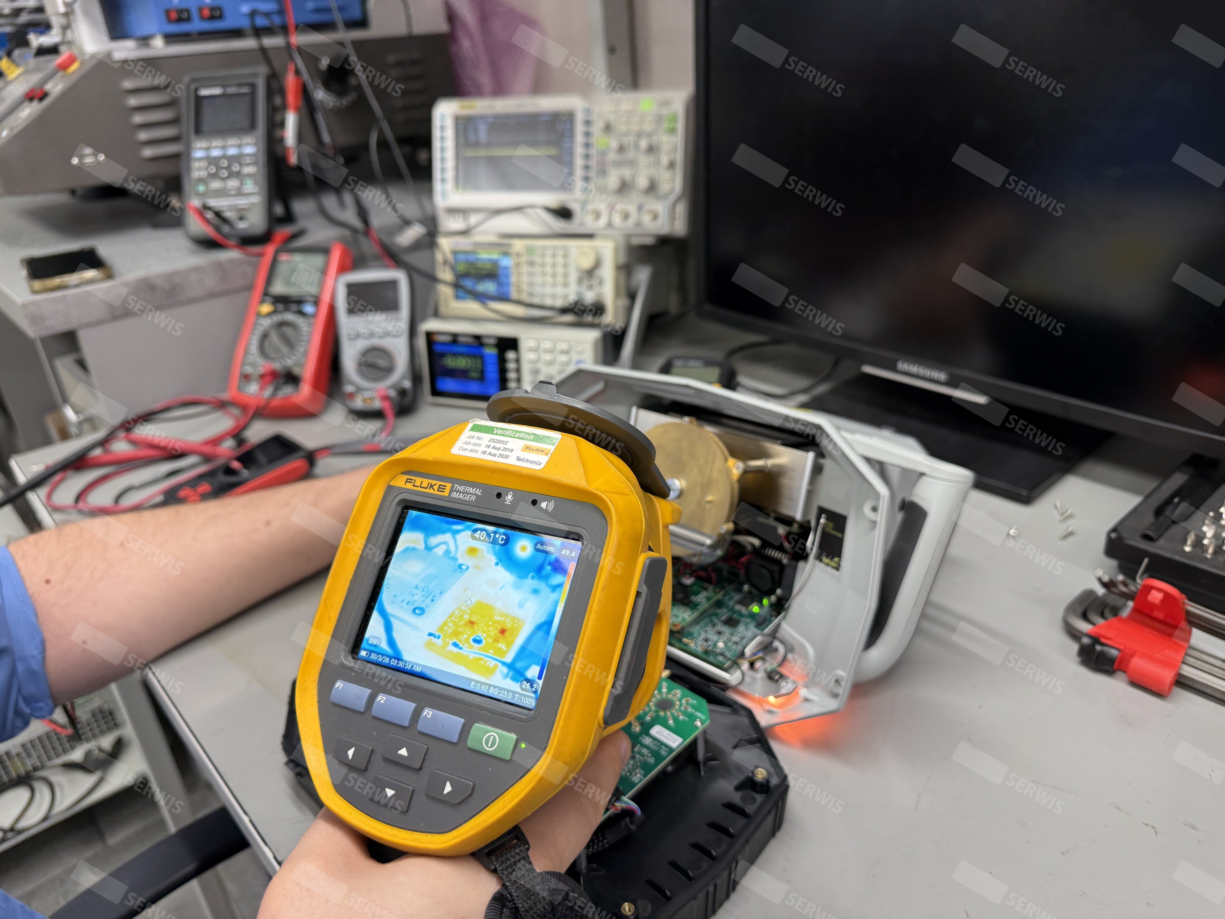
We use infrared diagnostics in our fault-analysis process. Thermal imaging is applied as a measurement tool, not a presentation aid.
It allows us to detect:
- overloads in power supply sections,
- asymmetry in converter operation,
- localized partial short circuits,
- abnormal operation of IGBT modules,
- degradation of power components,
- heat dissipation issues,
- discontinuities in conductive connections.
Our measurement procedures were developed based on controlled test setups and analysis of parameters such as emissivity, ambient temperature, reflections, and load conditions. This method is particularly effective for high-power industrial equipment, which can be examined under real operating conditions.
Development of Thermal Imaging Diagnostic Procedures
As early as 2013, in cooperation with Wrocław University of Science and Technology, we took part in a research project on the use of thermal imaging for non-contact diagnostics of electronic equipment. At a time when thermal imaging was not yet widely used in industrial electronics service, we developed practical measurement procedures designed for real-world service conditions. These methods were incorporated into our diagnostic procedures and remain a valuable tool supporting fault analysis in industrial electronics to this day. Below we present material outlining the project's objectives and examples of practical applications of thermal imaging diagnostics.

Endoscopic Inspection
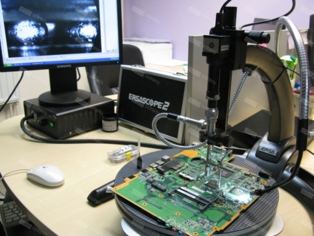
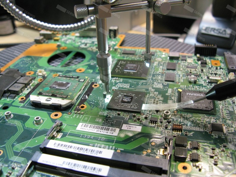
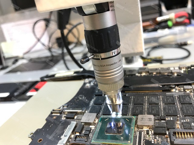
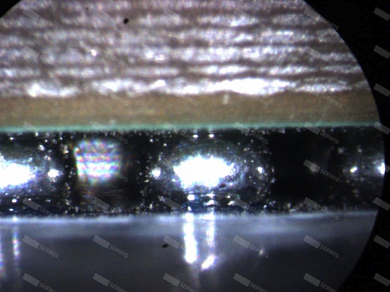
Endoscopic inspection is used to examine soldered connections in locations inaccessible to conventional microscopy.
This includes, among others:
- BGA, µBGA, and CSP packages,
- FLIP CHIP structures,
- connections beneath metal shields,
- areas with limited geometric access,
- critical power supply sections.
Inspection is performed:
- before reballing or component replacement,
- during fault-cause analysis,
- after soldering, to verify connection quality.
In modern high-integration packages, damage can occur not only between the component and the board, but also inside the package itself, between the die and the substrate. In such cases, visual inspection without the right equipment is insufficient.
Endoscopic inspection is an integral part of our diagnostic and quality-control procedure.
X-ray Inspection
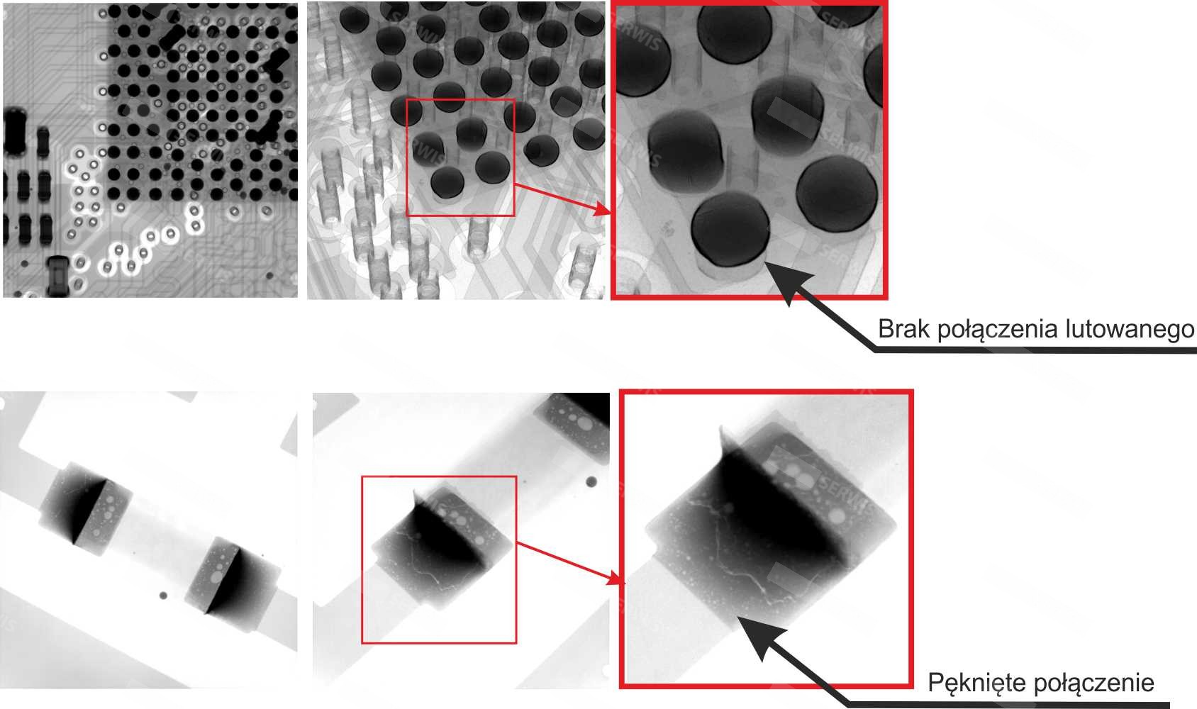
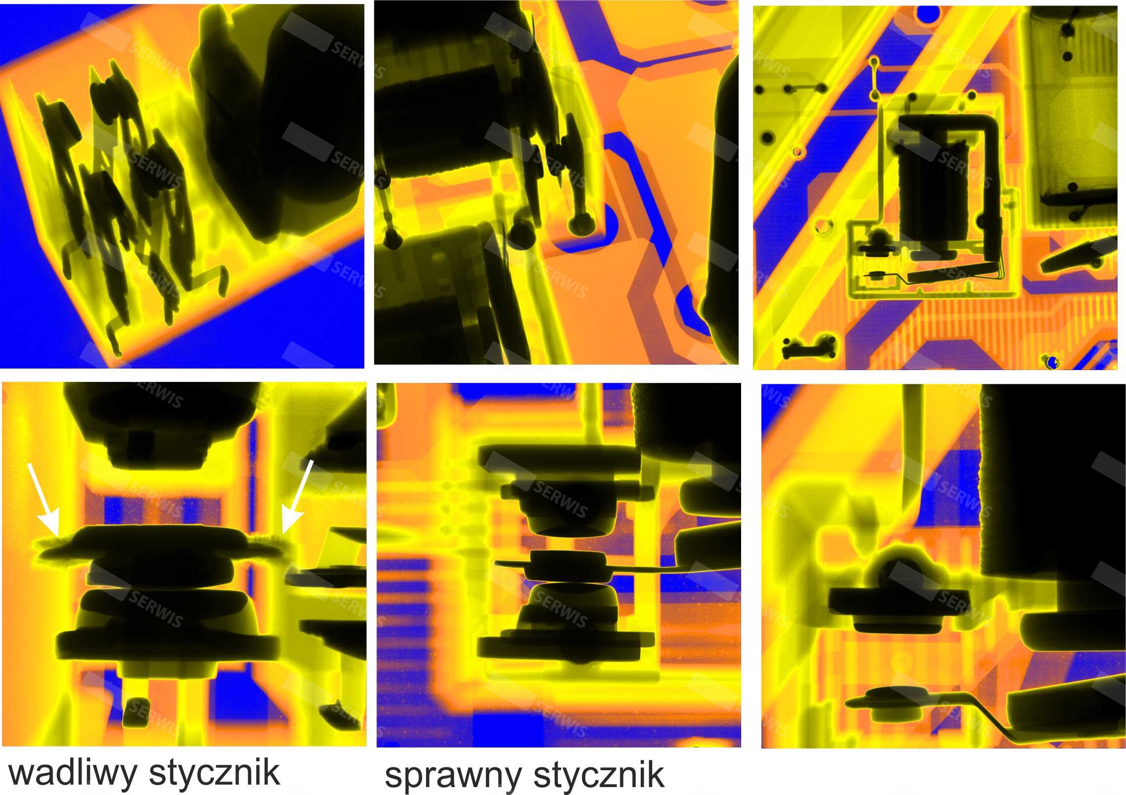
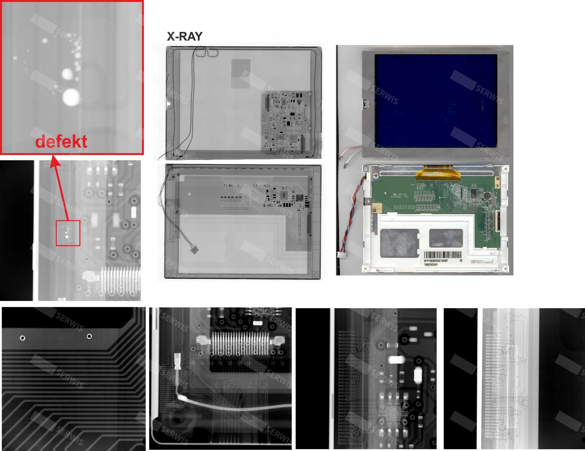
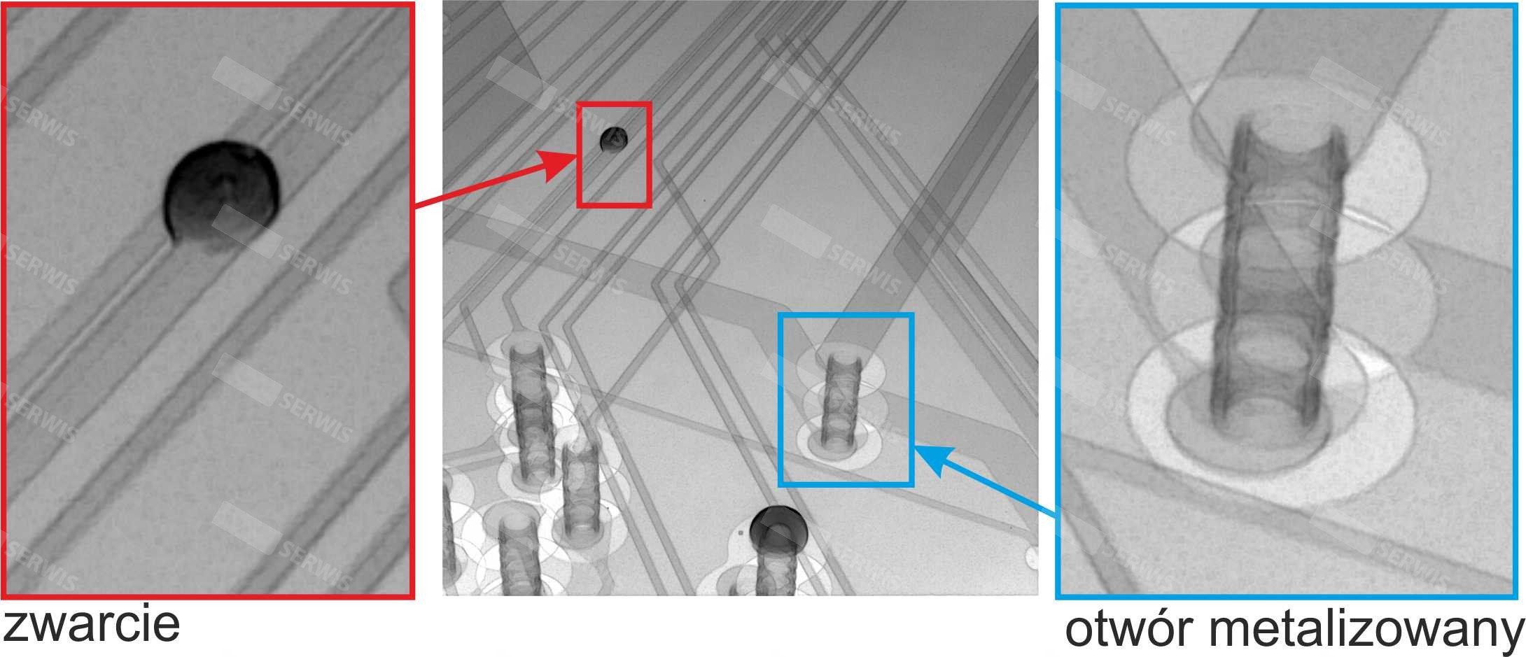
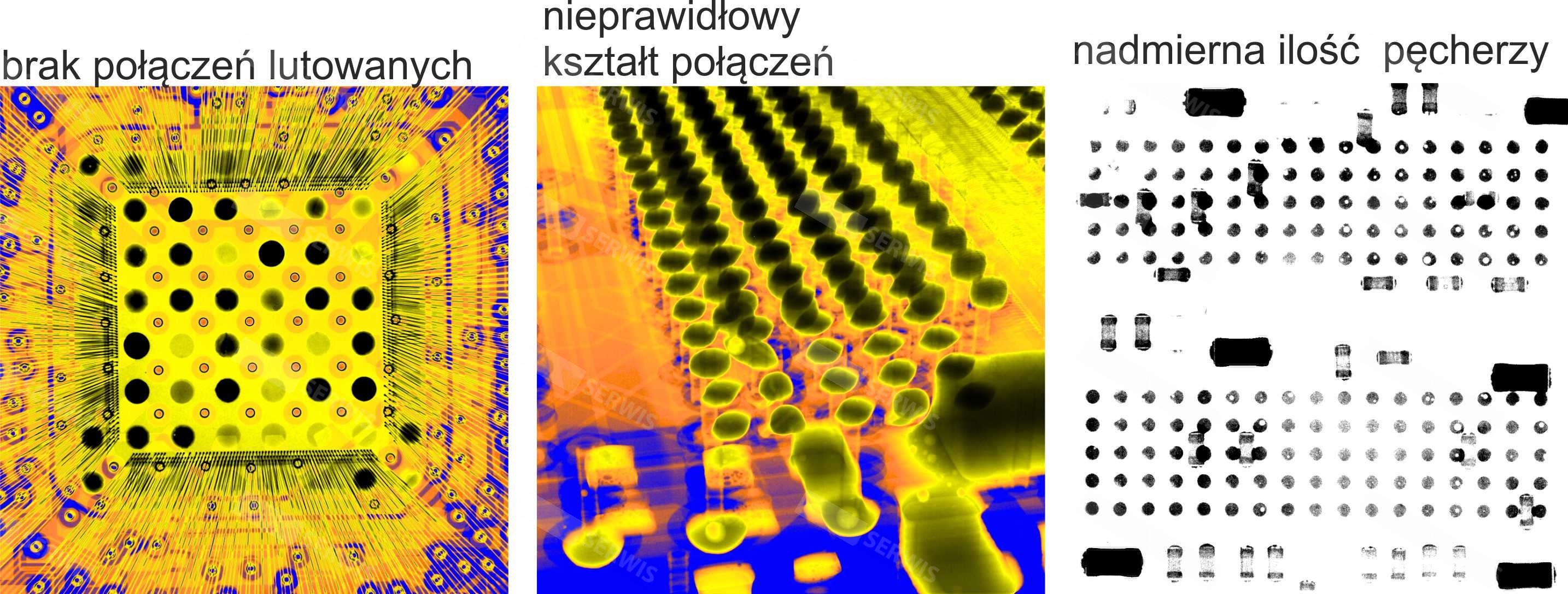
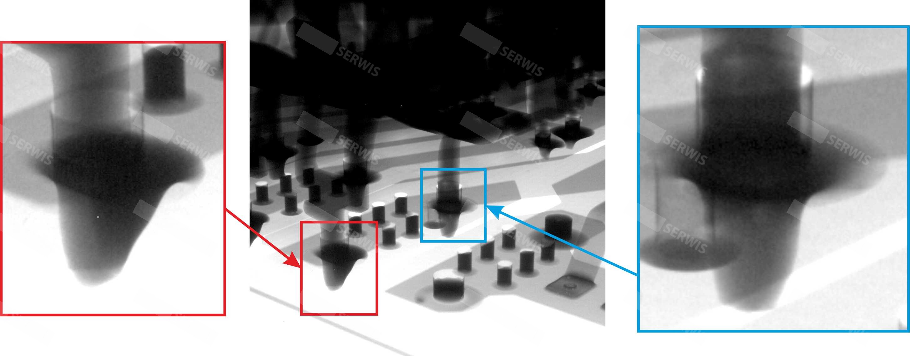
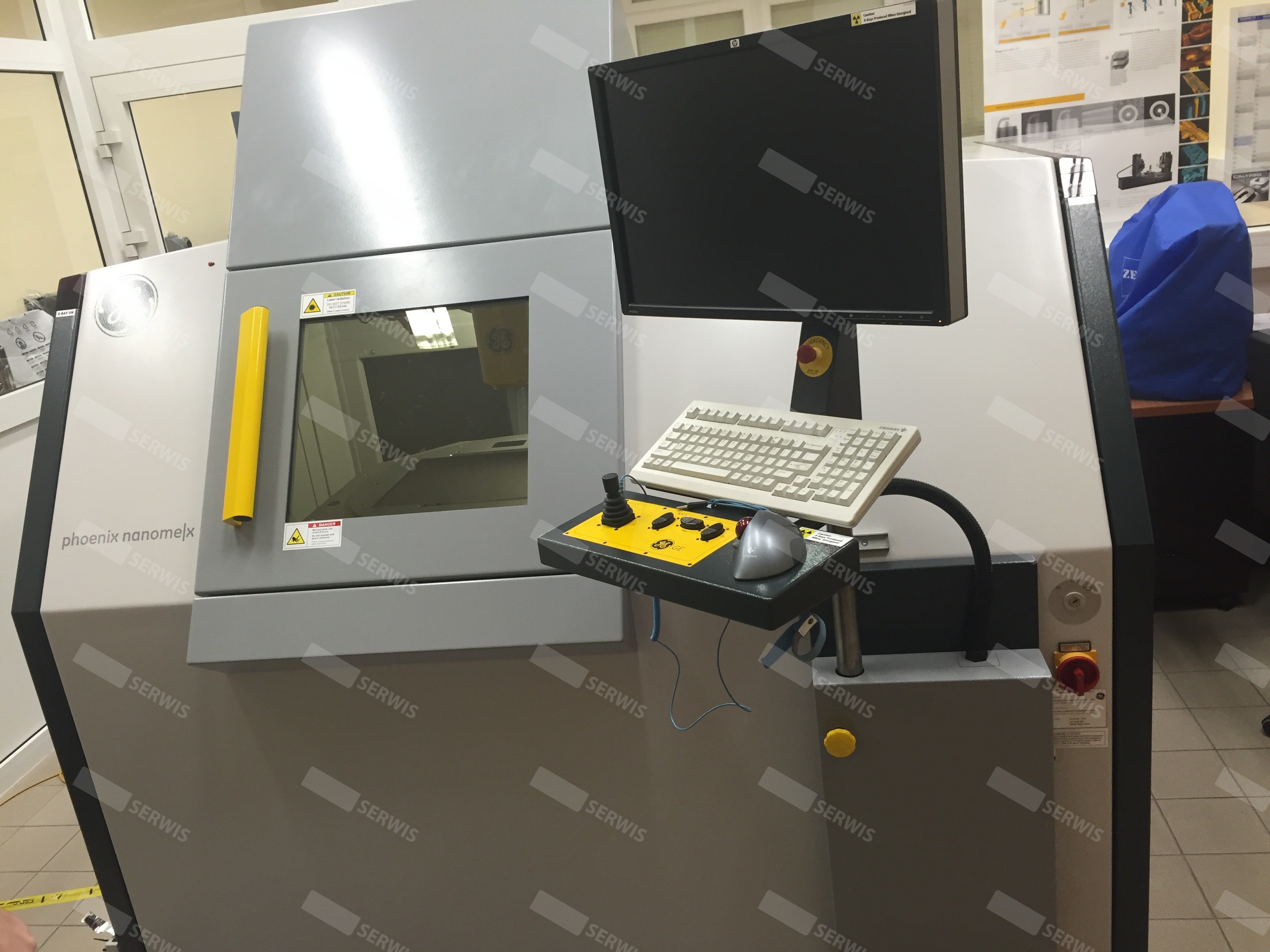
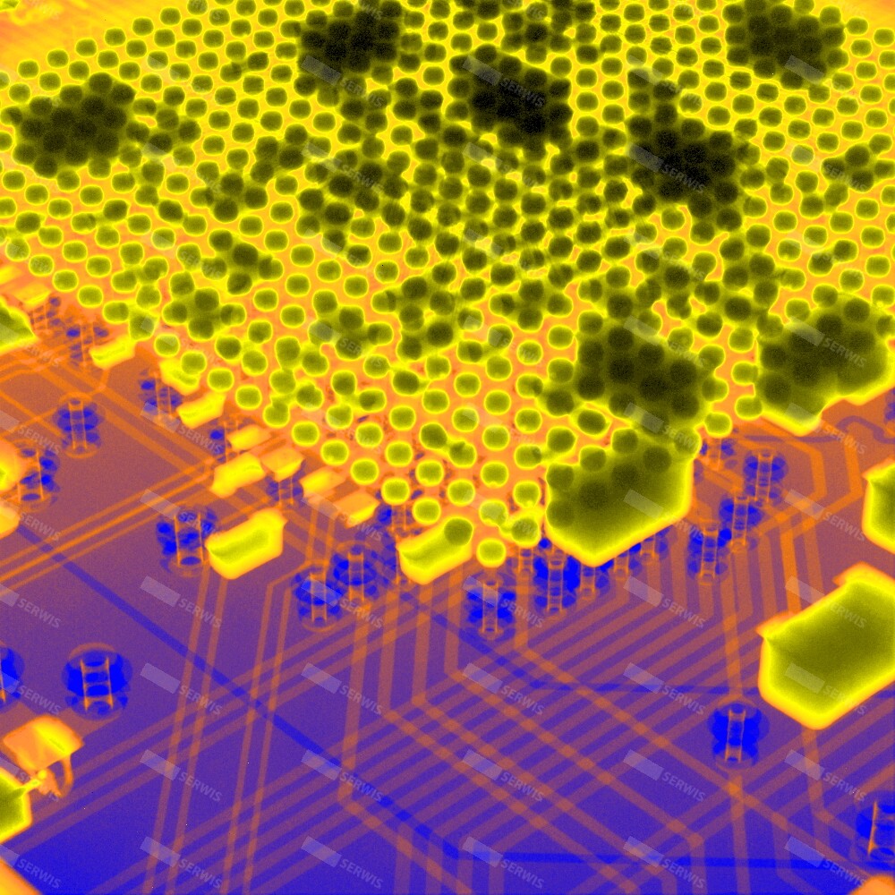
X-ray inspection is used whenever a full analysis of a component's internal structure is required.
It enables:
- assessment of connection quality beneath BGA packages,
- detection of voids and gaps within solder joints,
- analysis of solder bridges,
- inspection of multilayer structures,
- assessment of power component condition,
- analysis of mechanical wear in sealed components.
This technology is not limited to digital electronics.
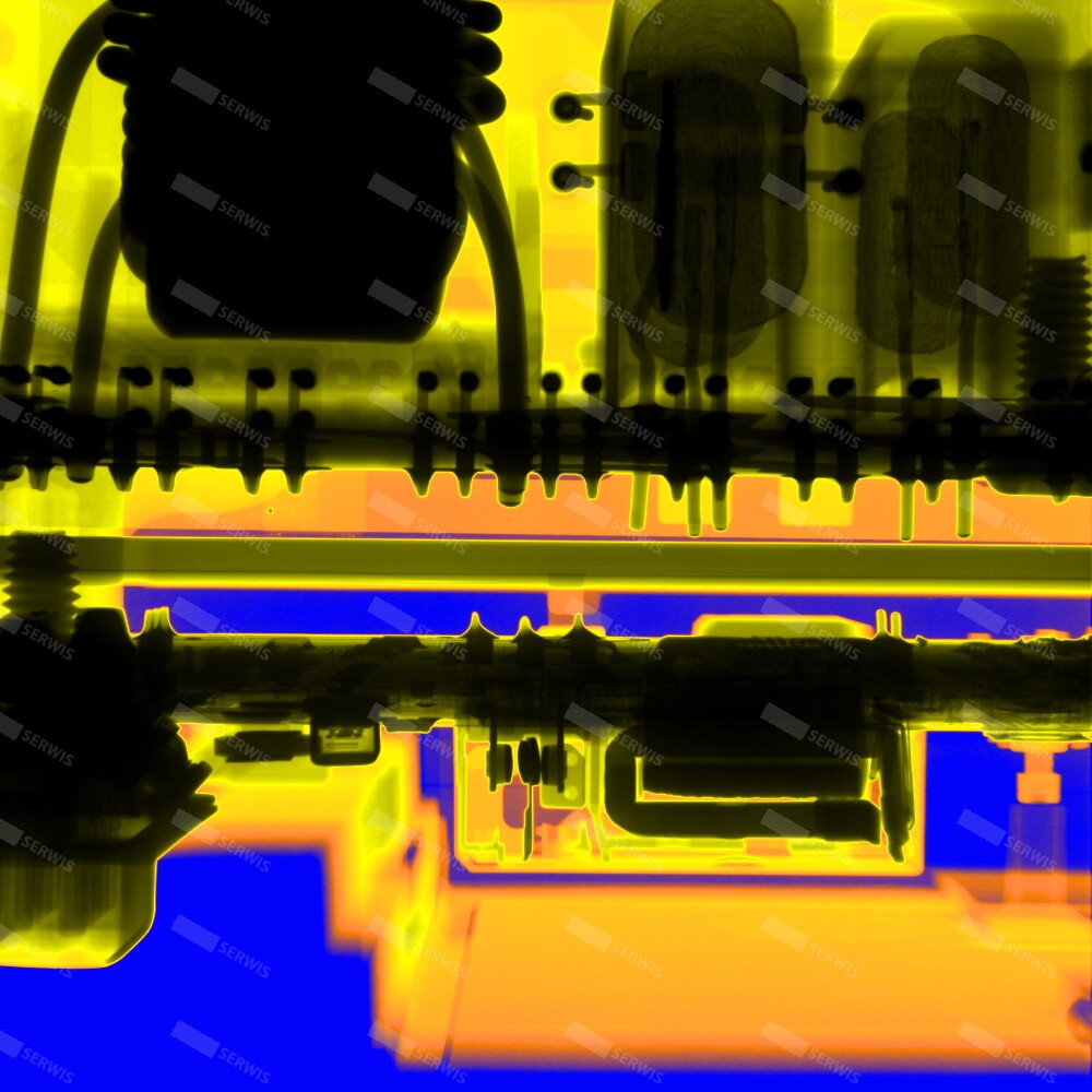
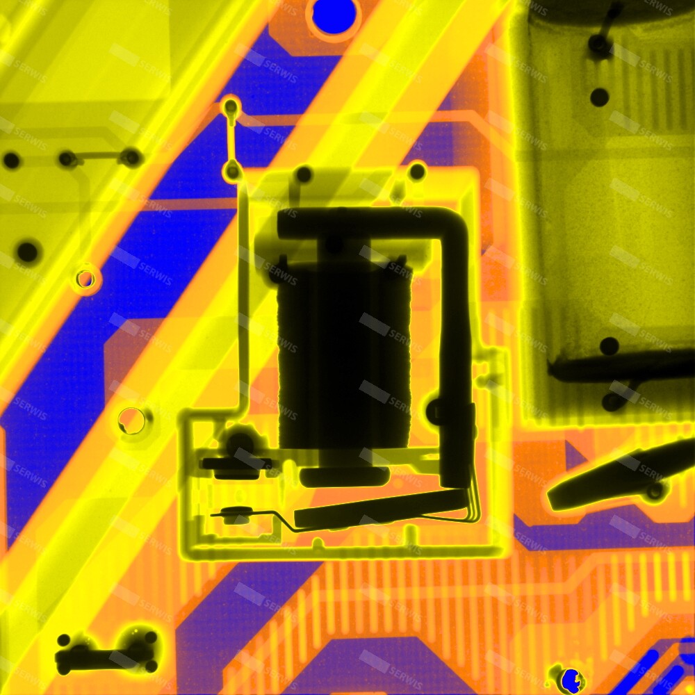
In practice, we also use it to assess the condition of electromechanical components, such as contactors and contact assemblies, where deformation or wear can be analyzed without disassembly. In uncertain cases, X-ray inspection confirms a diagnosis obtained through other methods.
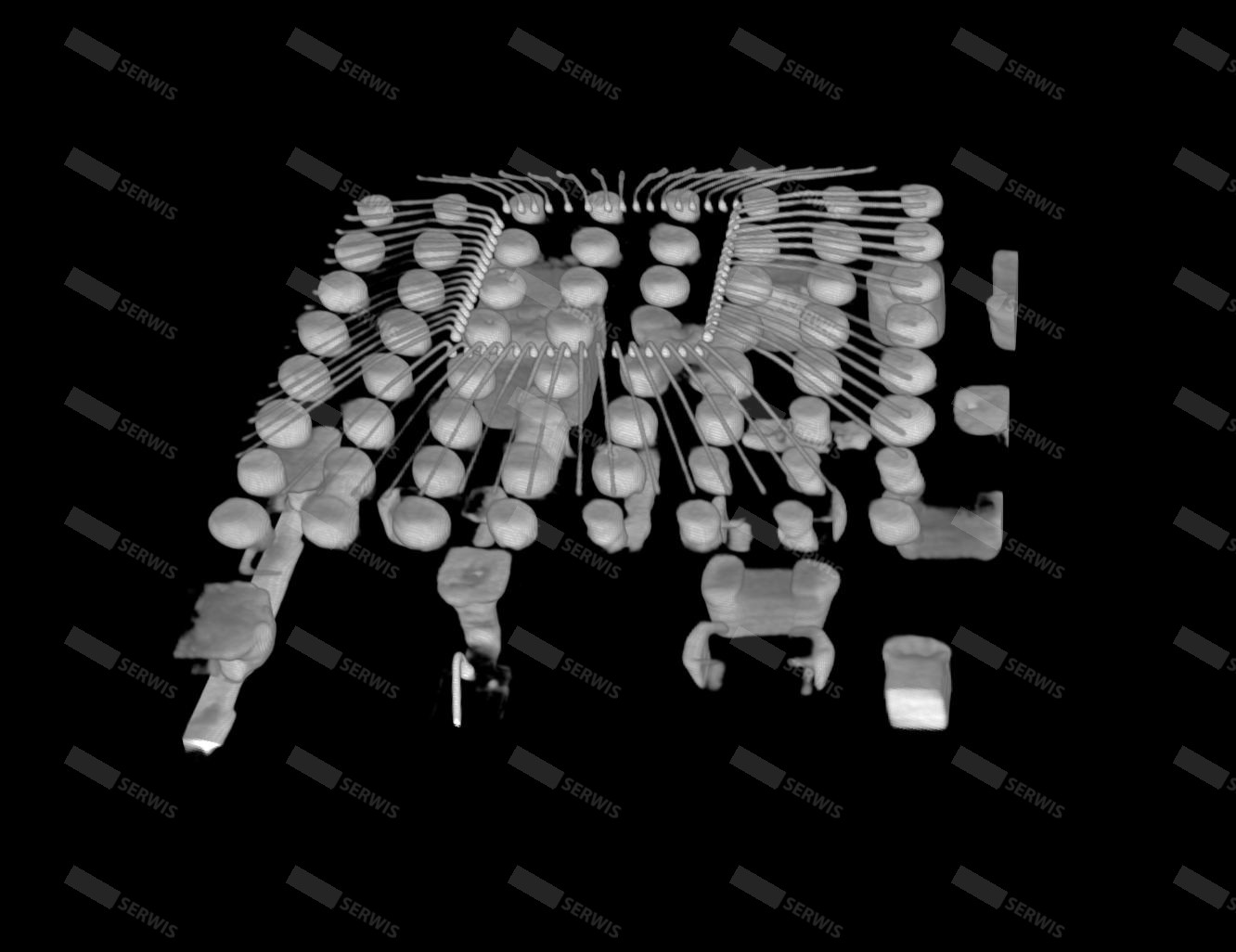
POD Computed Tomography
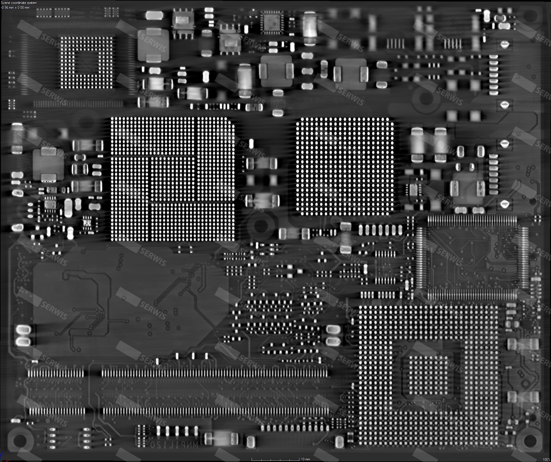
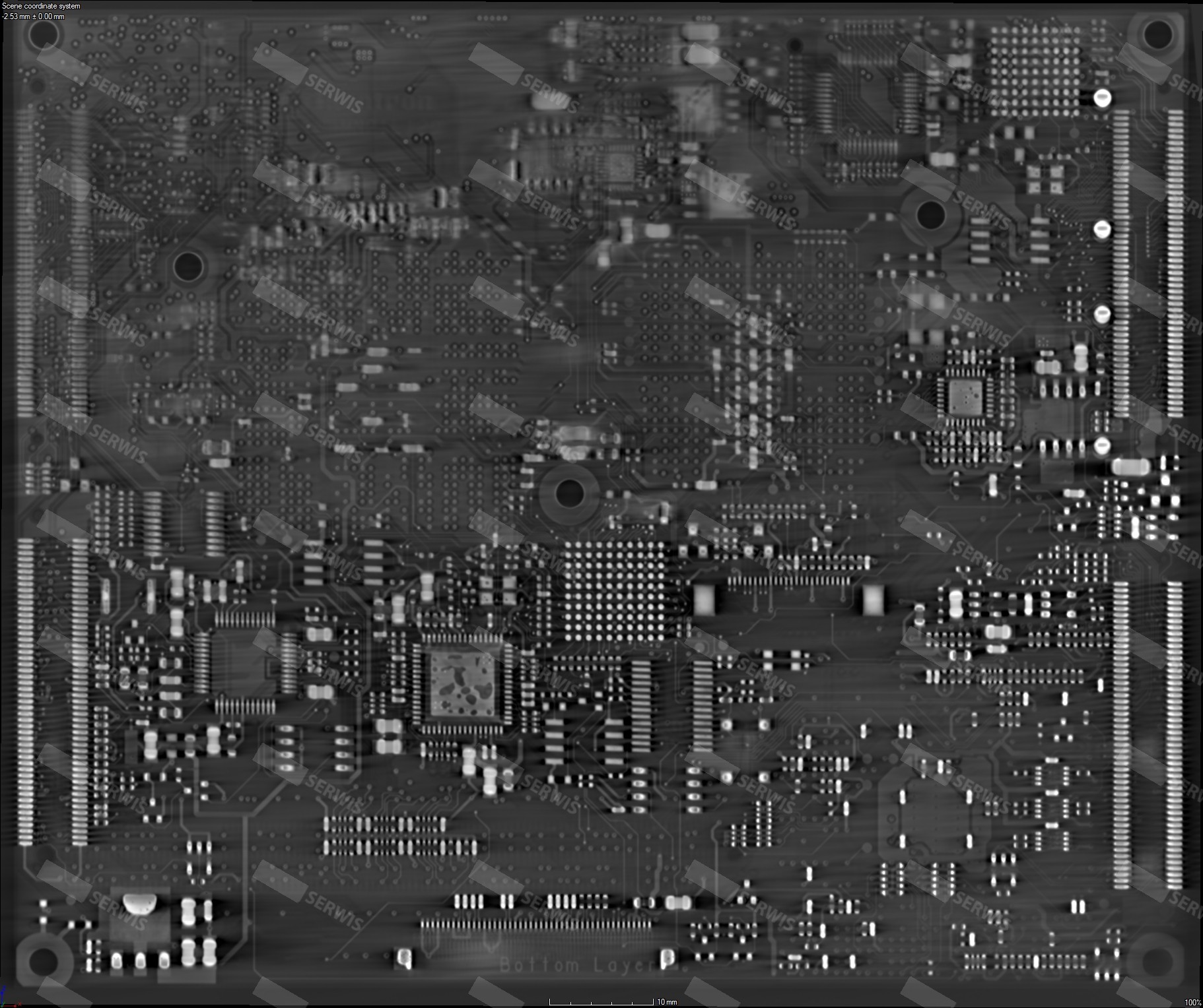
Computed tomography enables layer-by-layer analysis of printed circuit board structure without dismantling the device. Unlike conventional X-ray inspection, it allows precise tracing of printed circuit paths and localization of damage inside multilayer laminates.
This technology is applied primarily to complex electronic assemblies where standard diagnostic methods cannot conclusively identify the location of a fault.
Tomography makes it possible to:
- locate breaks in internal circuits,
- analyze the routing of connections within a multilayer PCB structure,
- identify short circuits between layers,
- assess the condition of vias and interlayer connections,
- verify that the actual structure matches the board documentation.
This method is especially valuable for modern industrial equipment, where faults often occur in structures invisible from the outside and cannot be detected by conventional electrical measurements. Tomography complements electrical diagnostics and X-ray inspection, increasing the effectiveness of locating complex and non-standard faults.
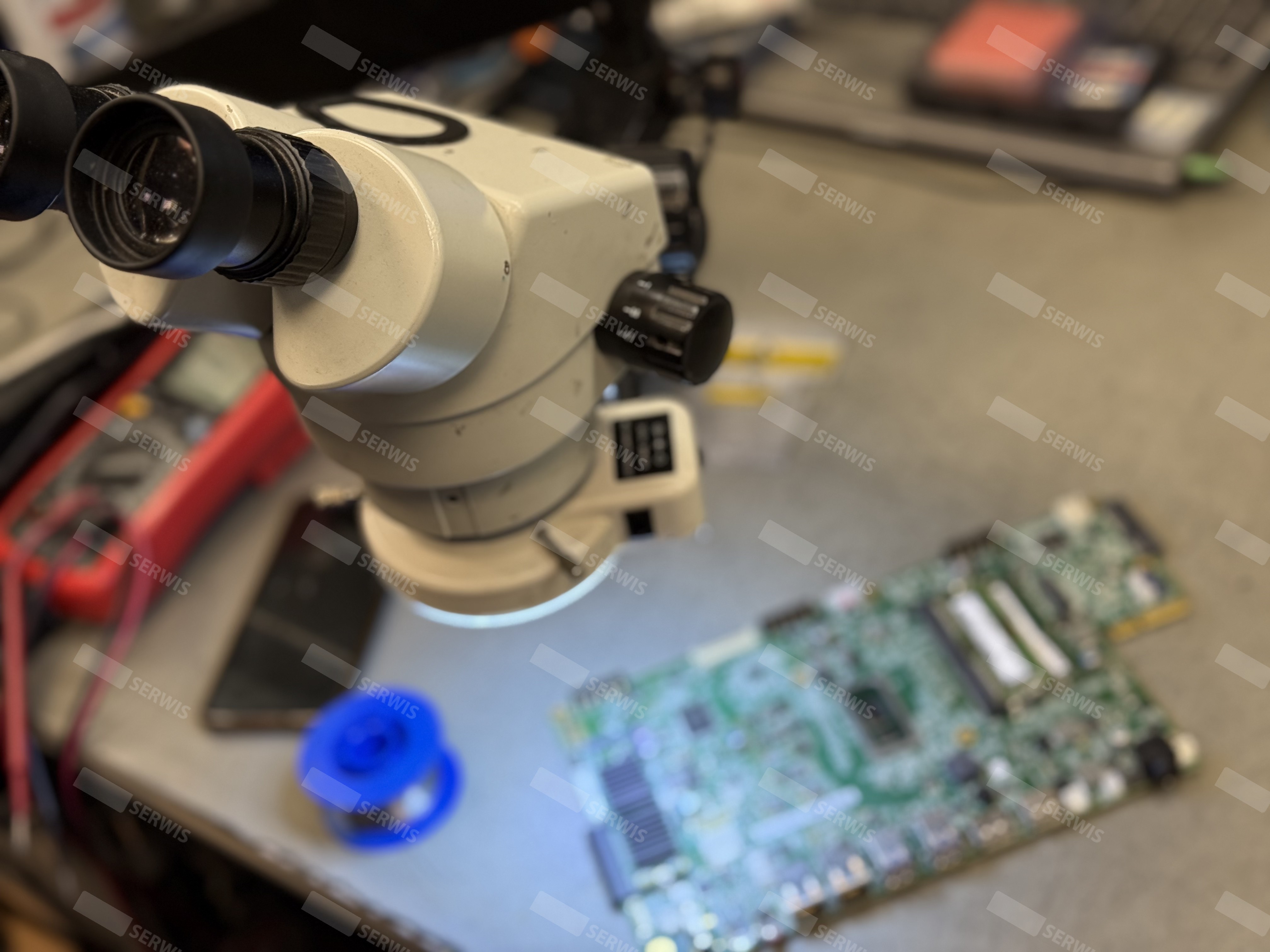
Microscopy and Multilayer Structure Repair
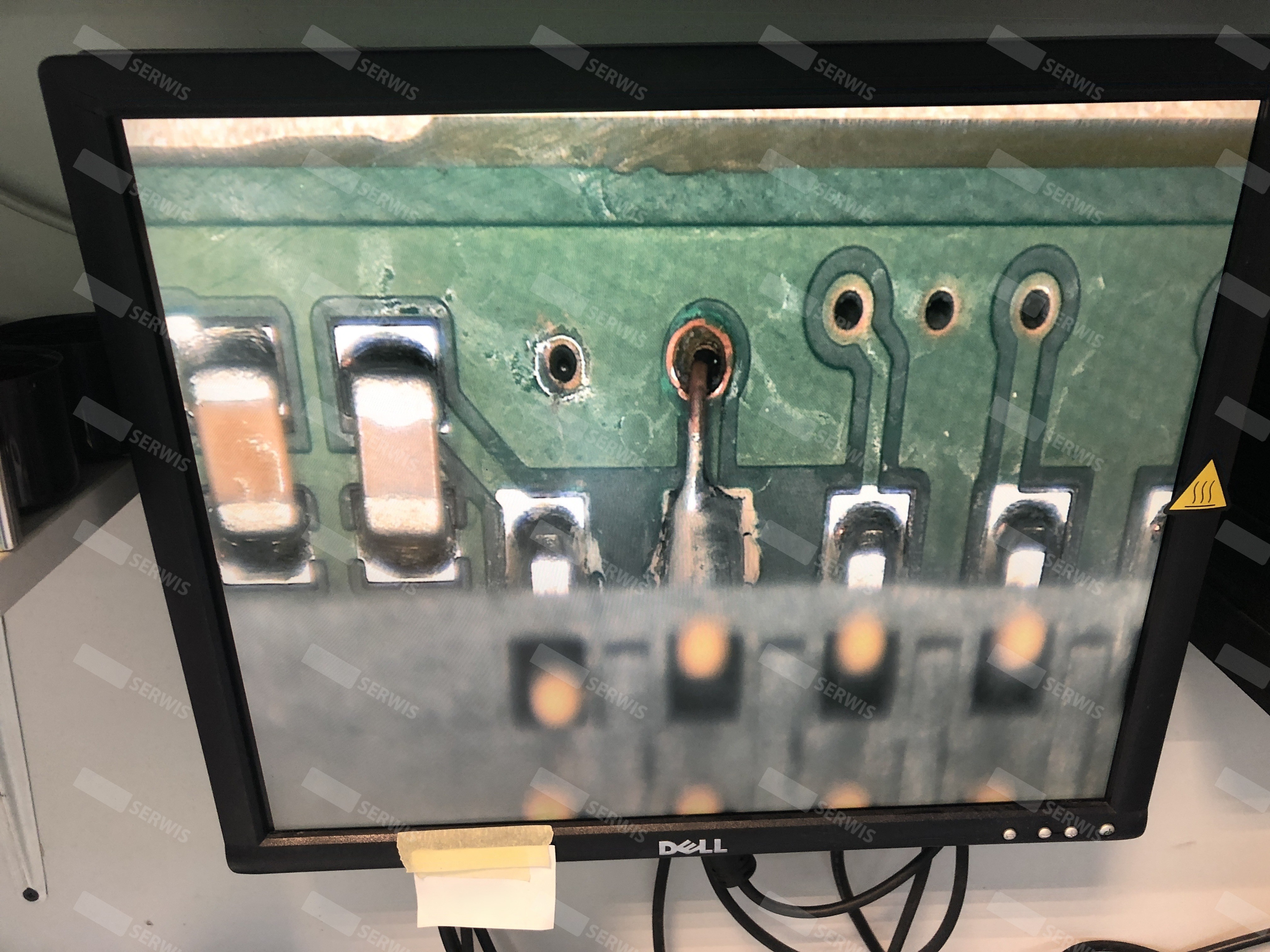
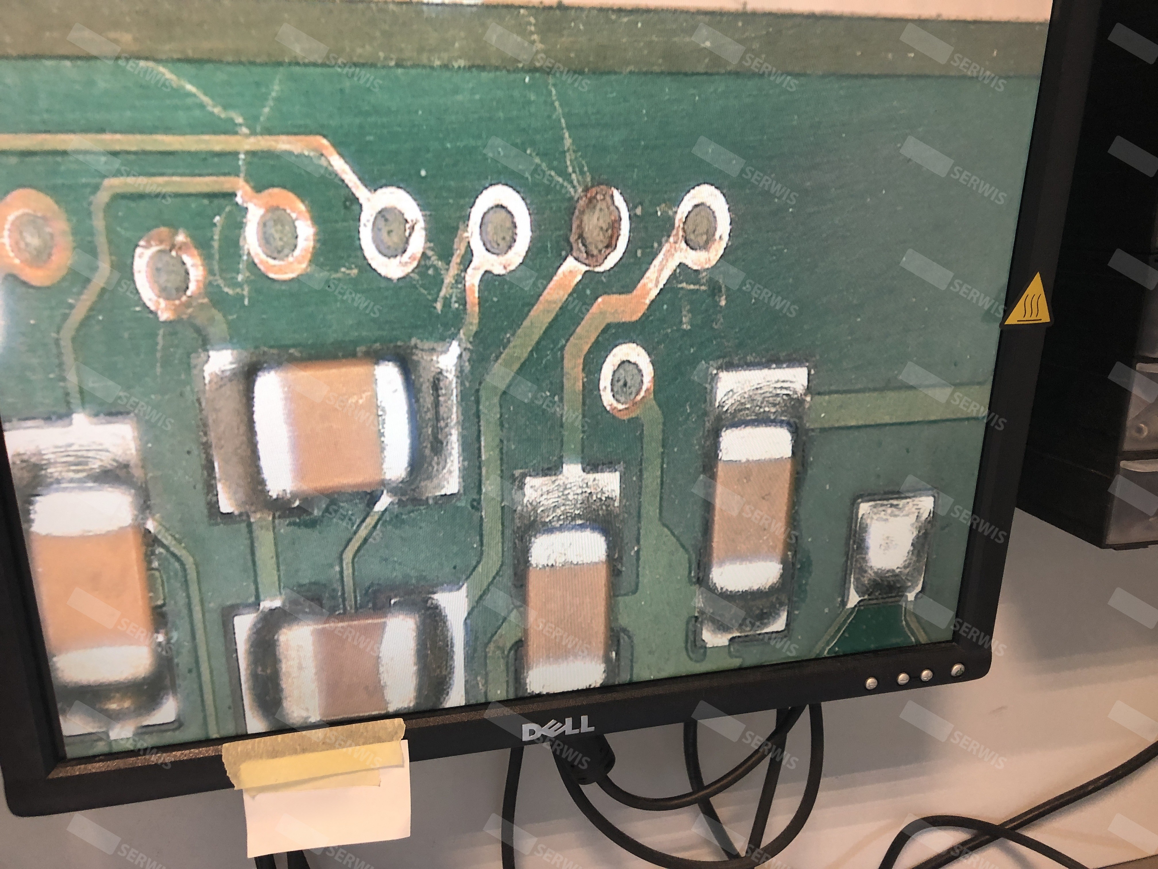
Our laboratory performs repairs that require intervention within the laminate structure itself.
This scope includes, among others:
- regeneration of interlayer vias,
- reconstruction of soldering pads,
- repair of damaged printed circuits,
- reconstruction of power supply sections,
- repair of mechanical PCB damage.
Modern industrial laminates consist of multiple layers and require a precise technological approach. Incorrect intervention can permanently damage the board structure.
Soldering and Reballing Technology
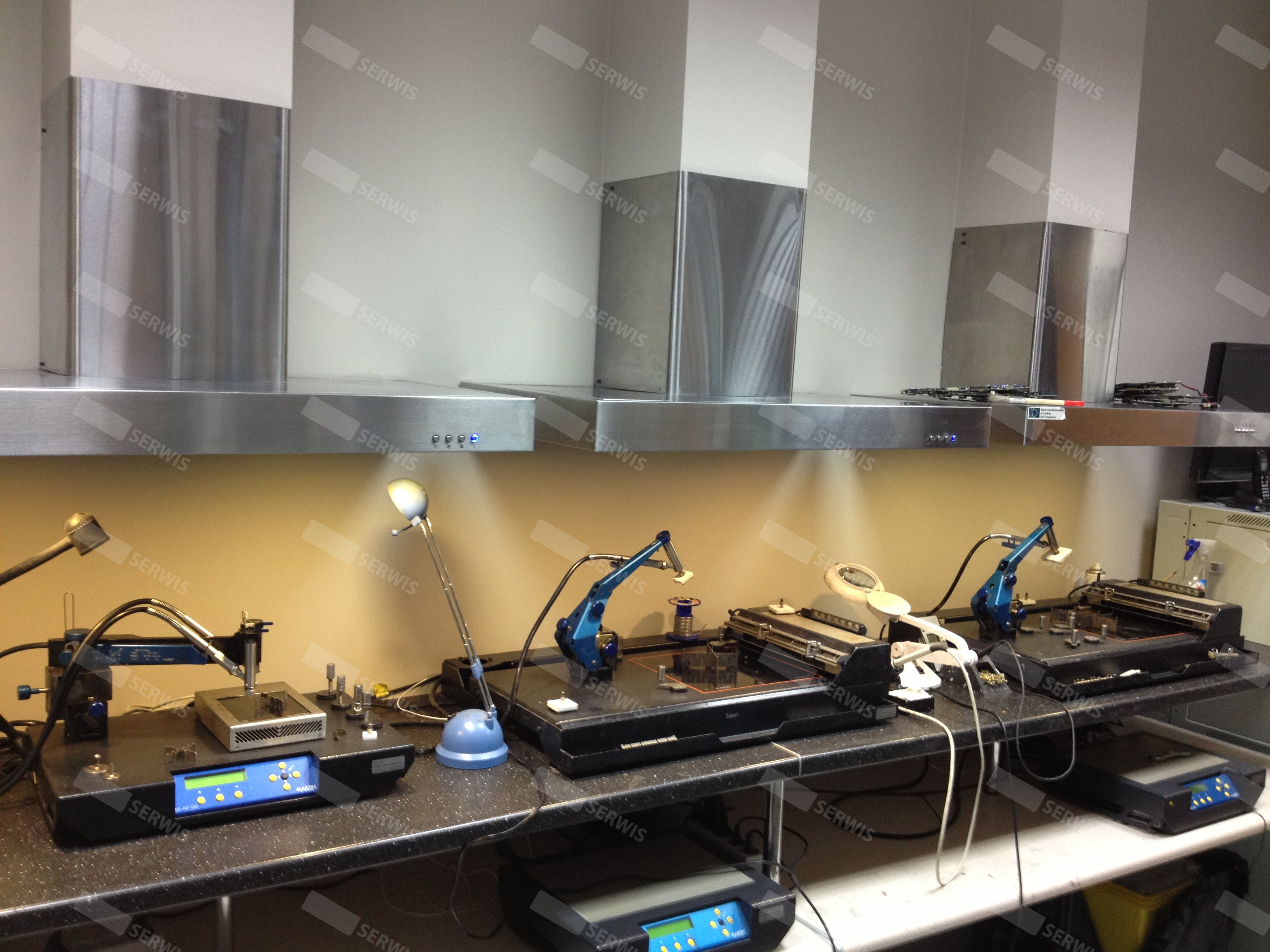
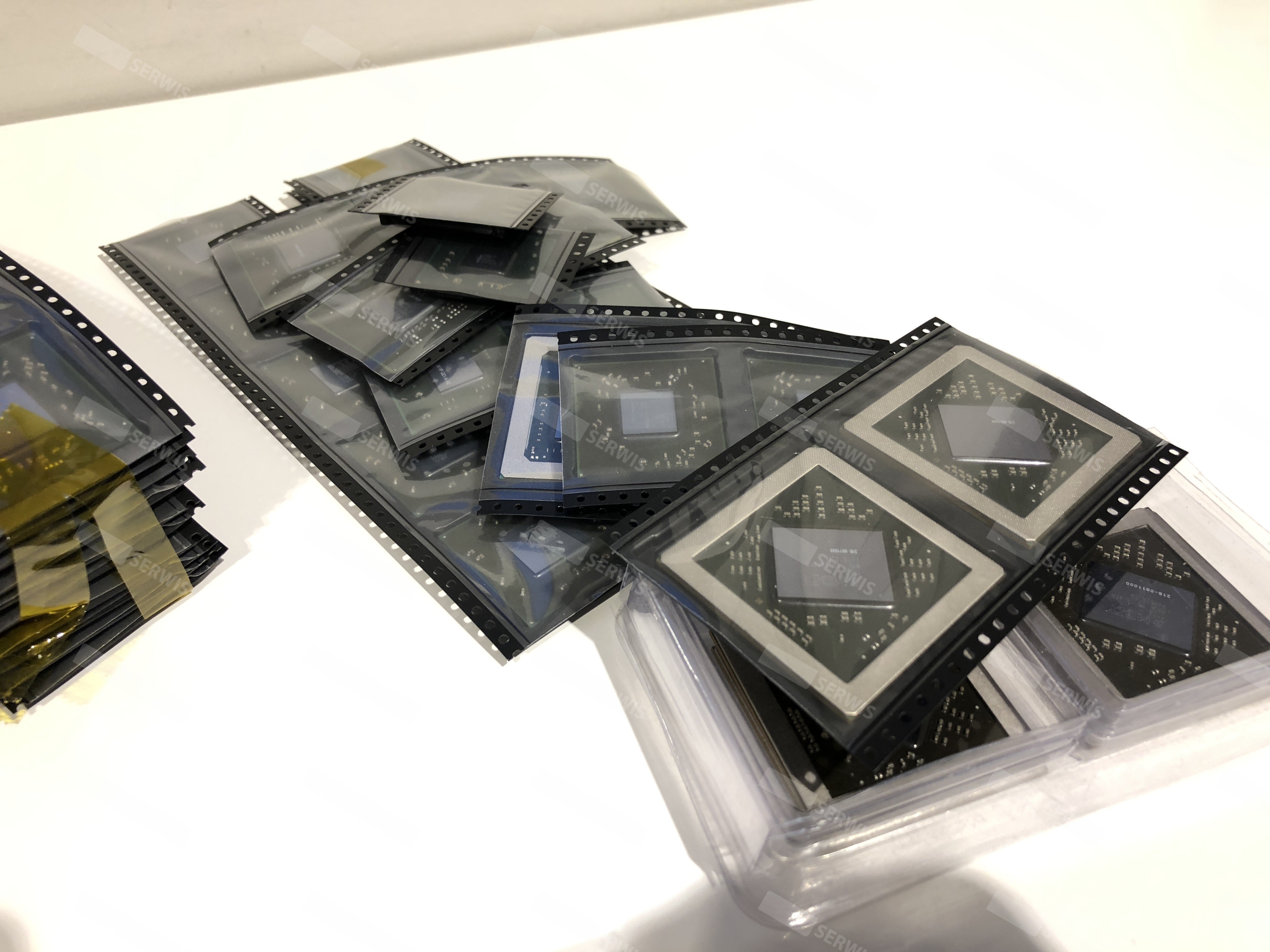
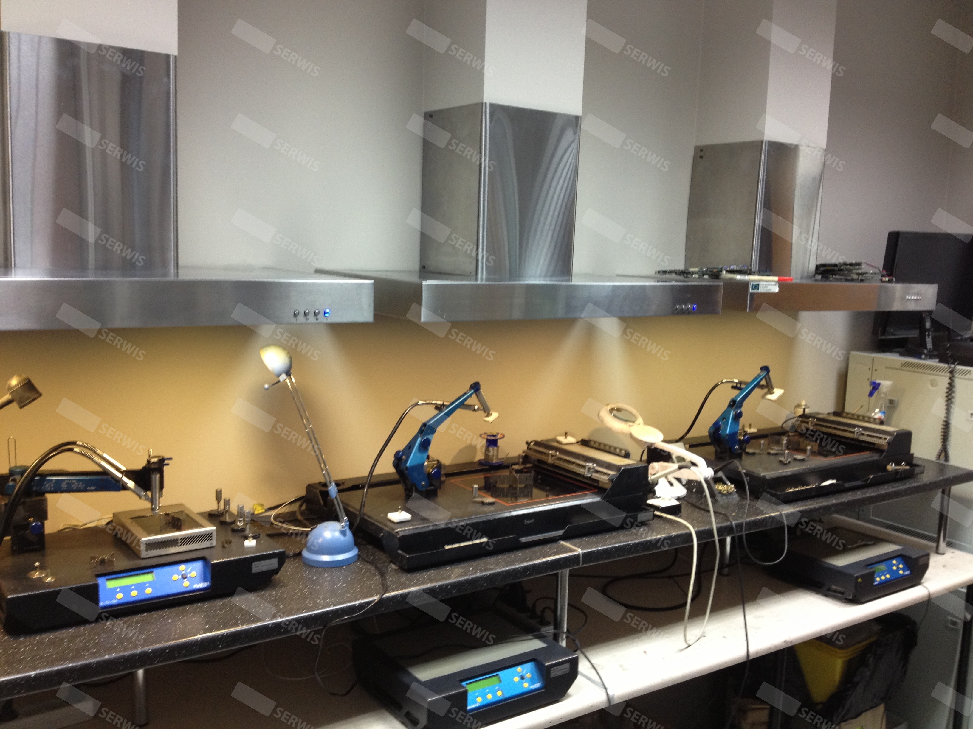
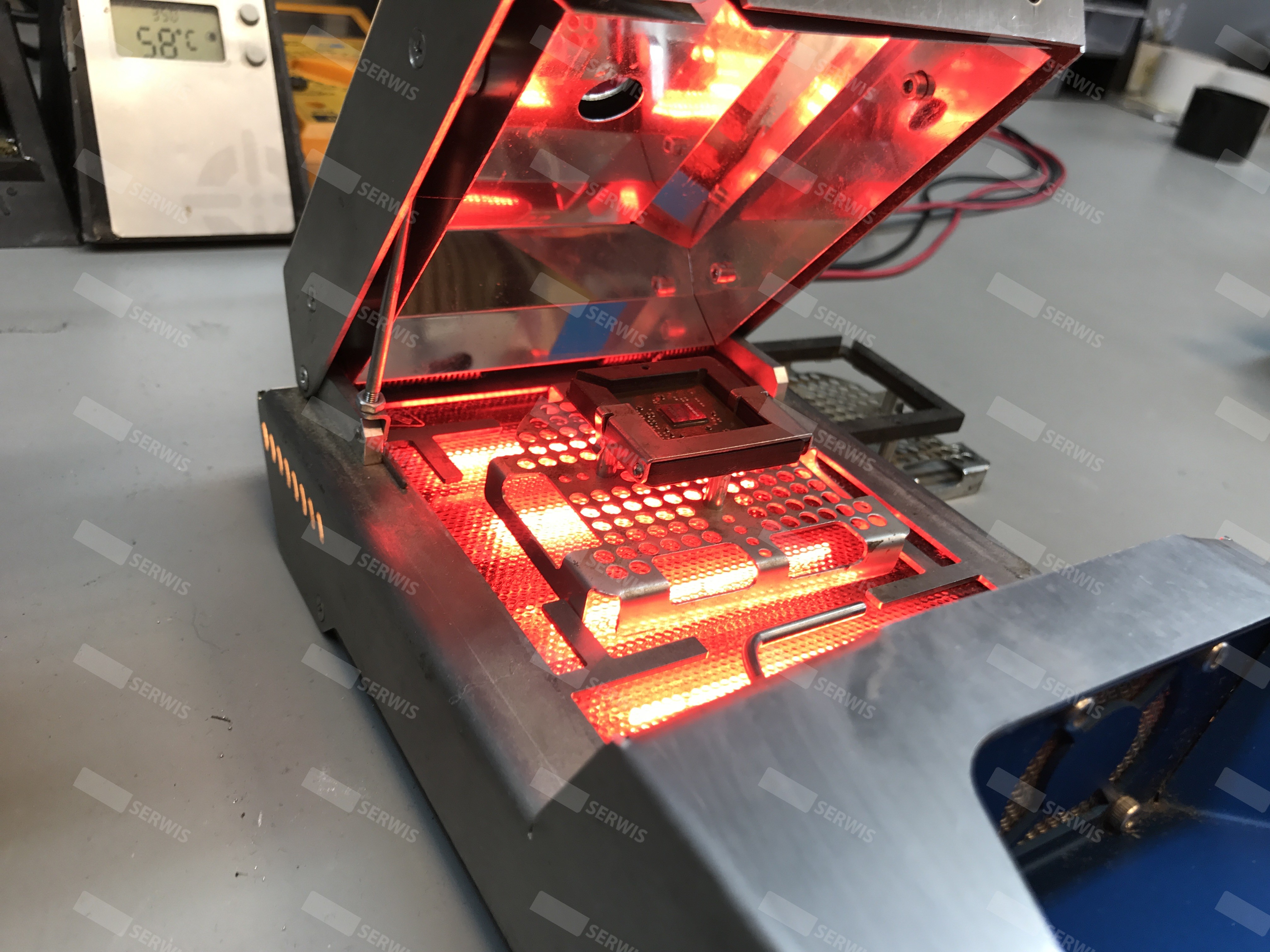
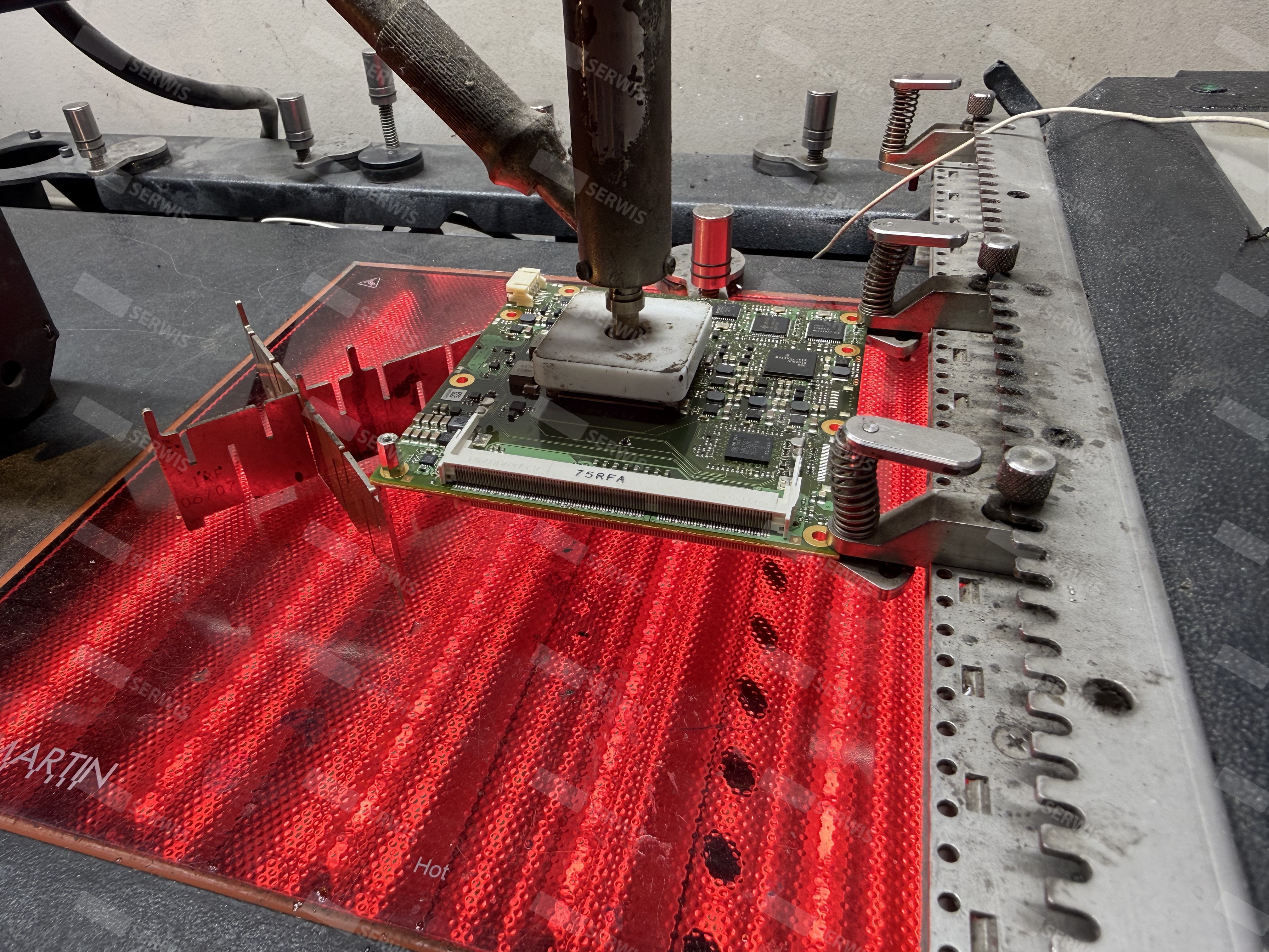
Repairs of SMD, QFP, BGA, µBGA, CSP, and FLIP CHIP packages are carried out using professional soldering systems with controlled temperature profiles.
The process includes:
- precise temperature control,
- control of thermal gradients,
- minimization of stress within the laminate structure,
- verification of connection quality once the process is complete.
During repairs, we apply precisely controlled thermal profiles, essential when working with multilayer boards and BGA, µBGA, and CSP technologies.
Measurement Facilities and Test Stations
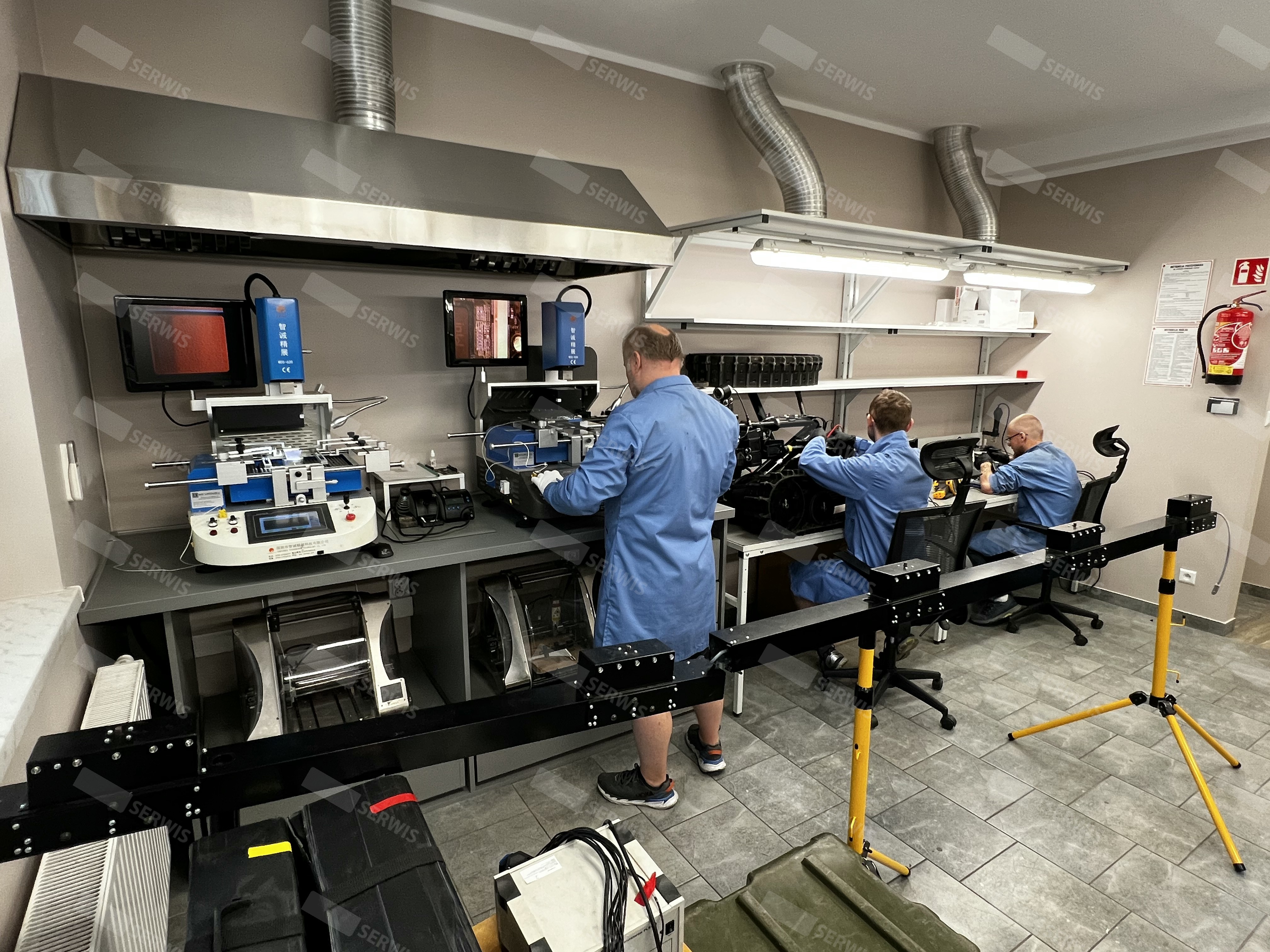
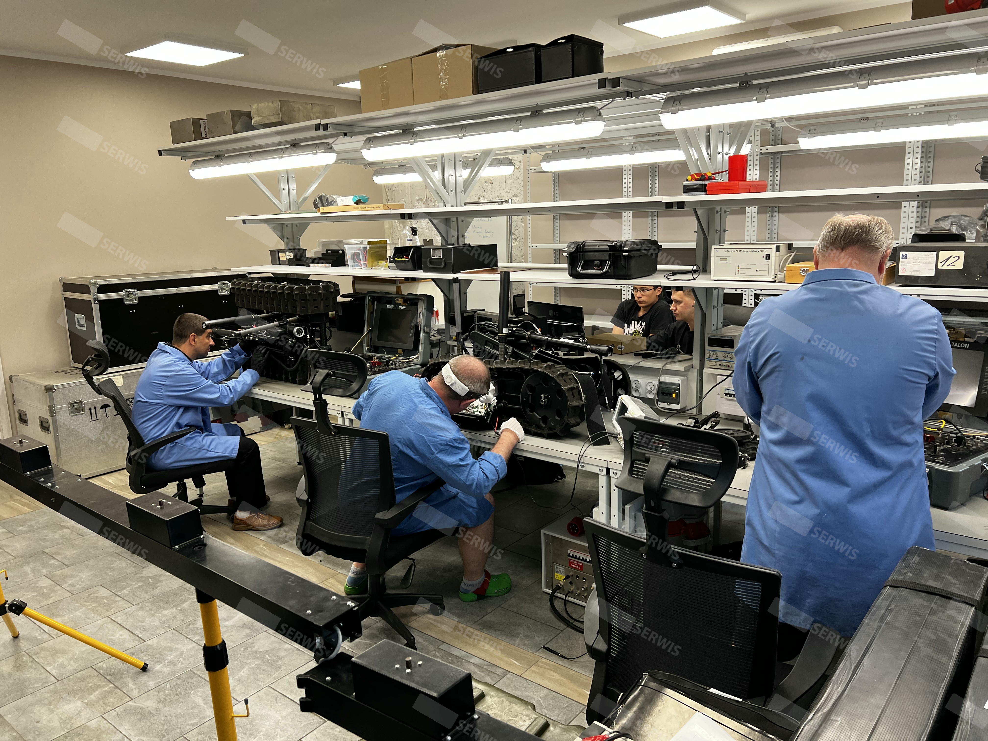
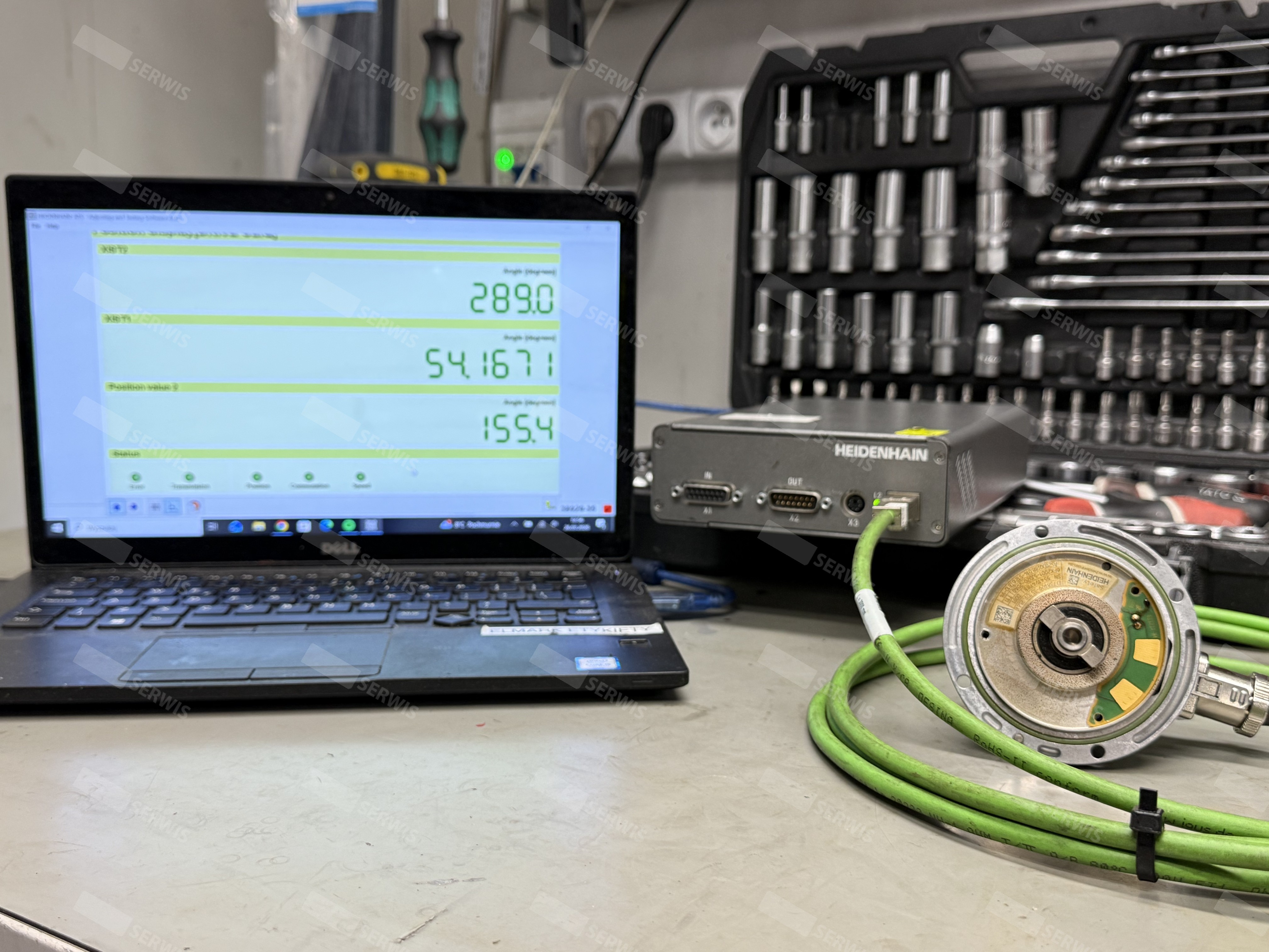
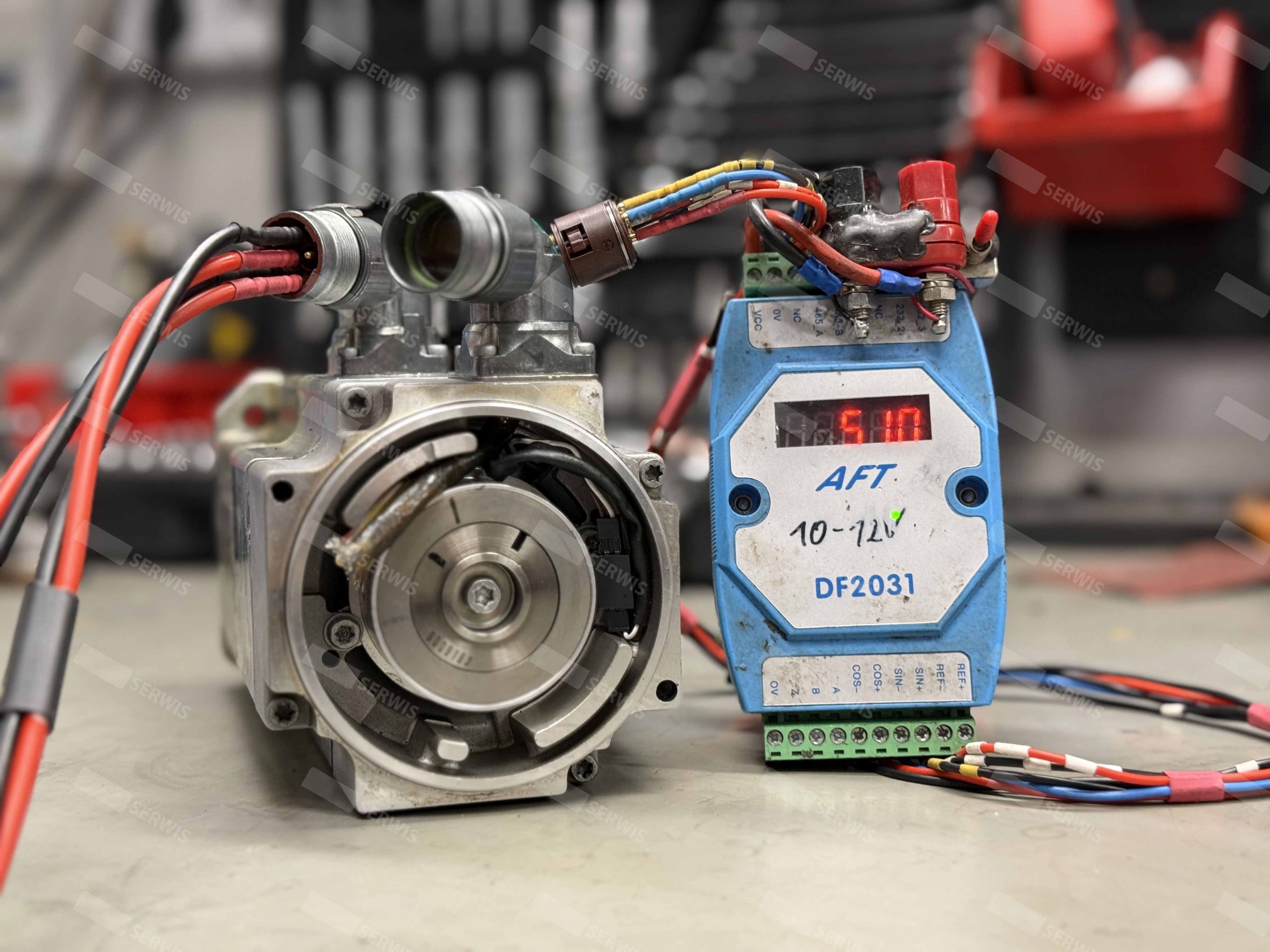
Diagnostics are supported by an extensive measurement facility, including:
- high-end digital oscilloscopes,
- dynamic-parameter meters,
- signal analyzers,
- calibrators,
- memory programmers,
- load test stations for power equipment,
- including measurement instruments from FLUKE and TEKTRONIX.
The company has an independent high-power electrical connection, enabling industrial equipment to be tested under real load conditions. Standard units are commissioned under laboratory conditions. For non-standard systems or high-power installations, final testing can be carried out directly at the customer's site.
Scientific Collaboration
Some of our diagnostic procedures were developed in collaboration with Wrocław University of Science and Technology as part of research on heat dissipation analysis and fault diagnostics in high-power electronic structures. The aim of the research was to improve fault-location effectiveness and reduce the risk of recurrence.
Our Standard of Work
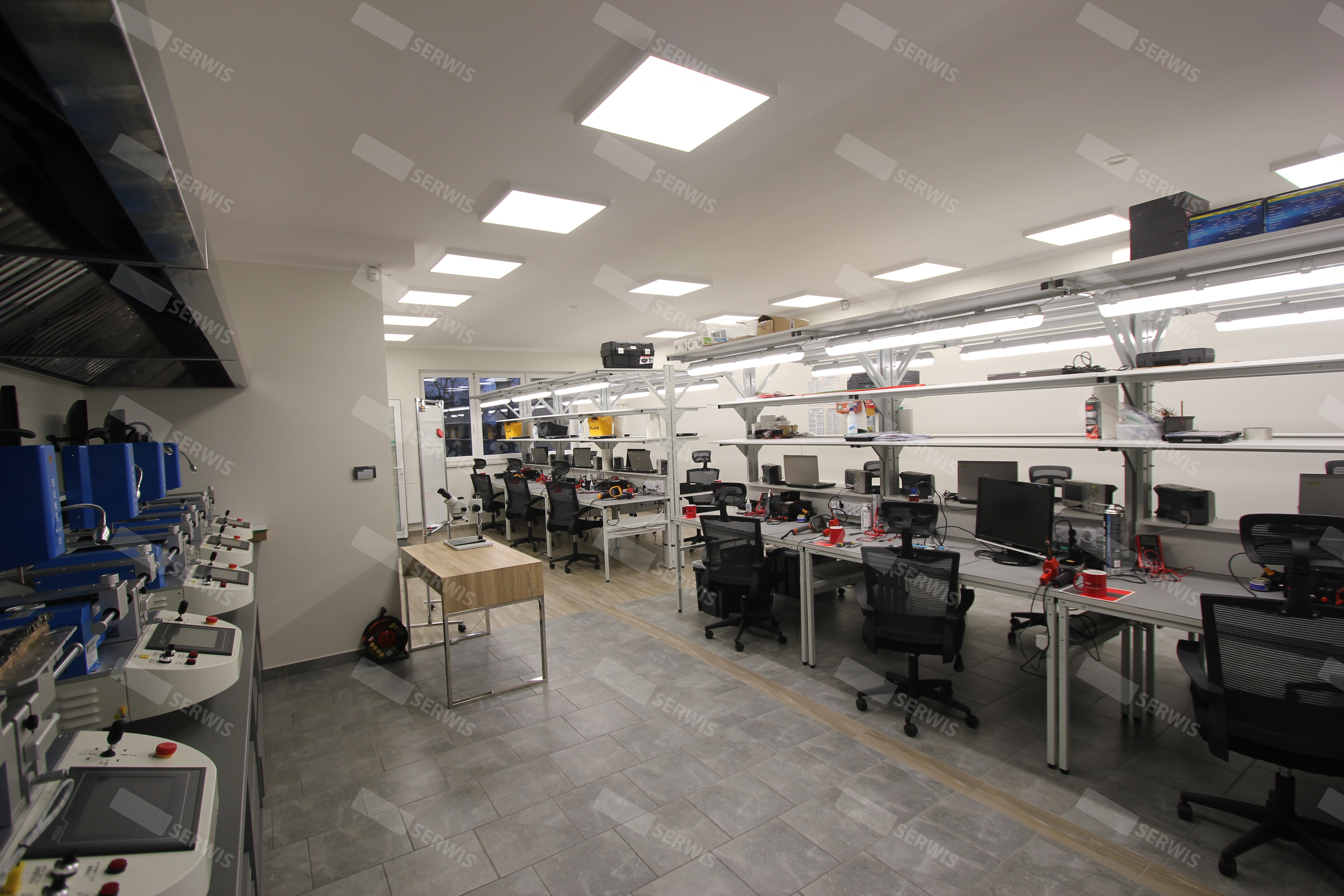
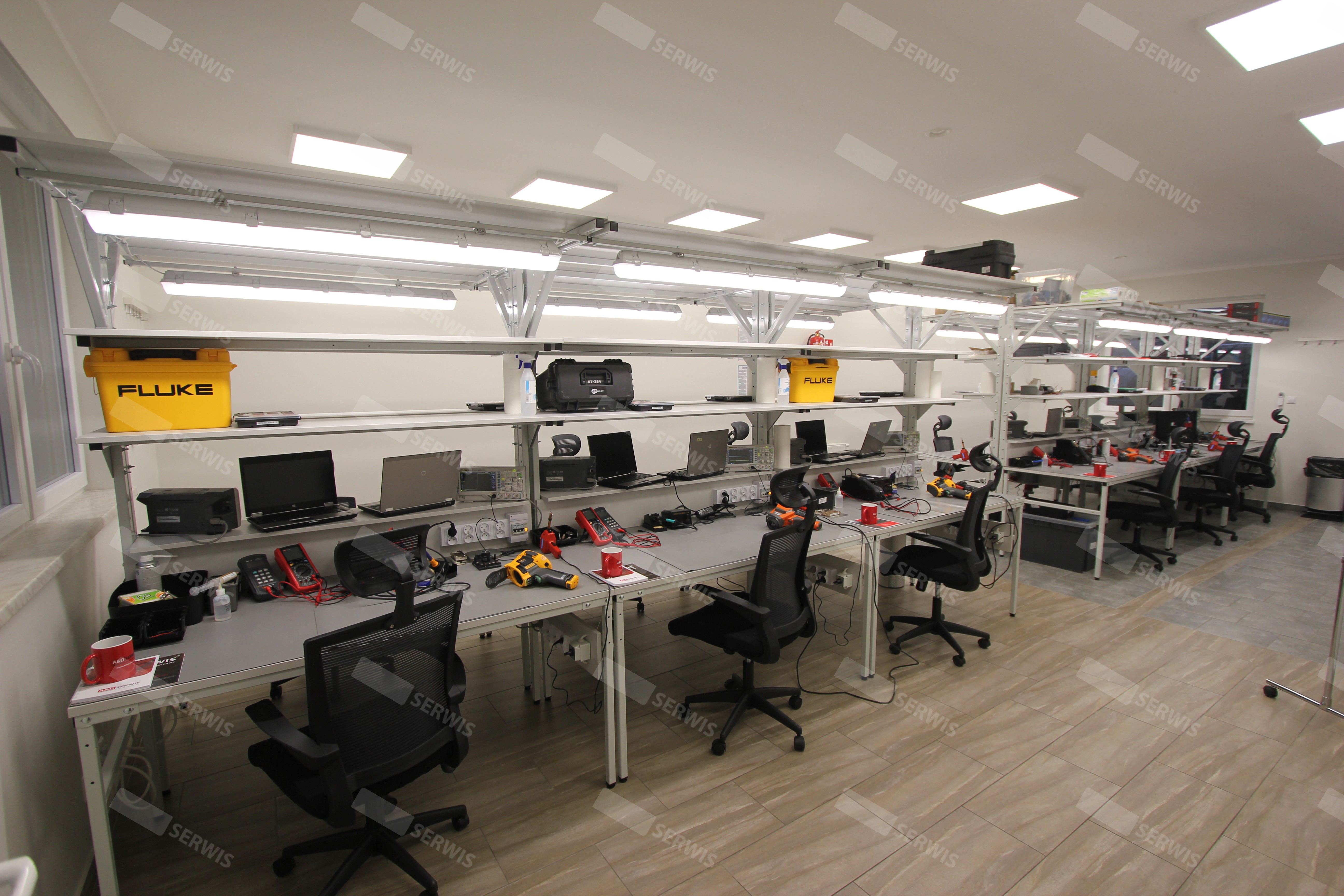
To us, a repair means analyzing the root cause of the failure, eliminating its effects, and verifying correct device operation before it is returned.
We do not limit ourselves to replacing entire modules when effective structural repair is possible. Every device undergoes full diagnostics, and the repair process follows established technical procedures.
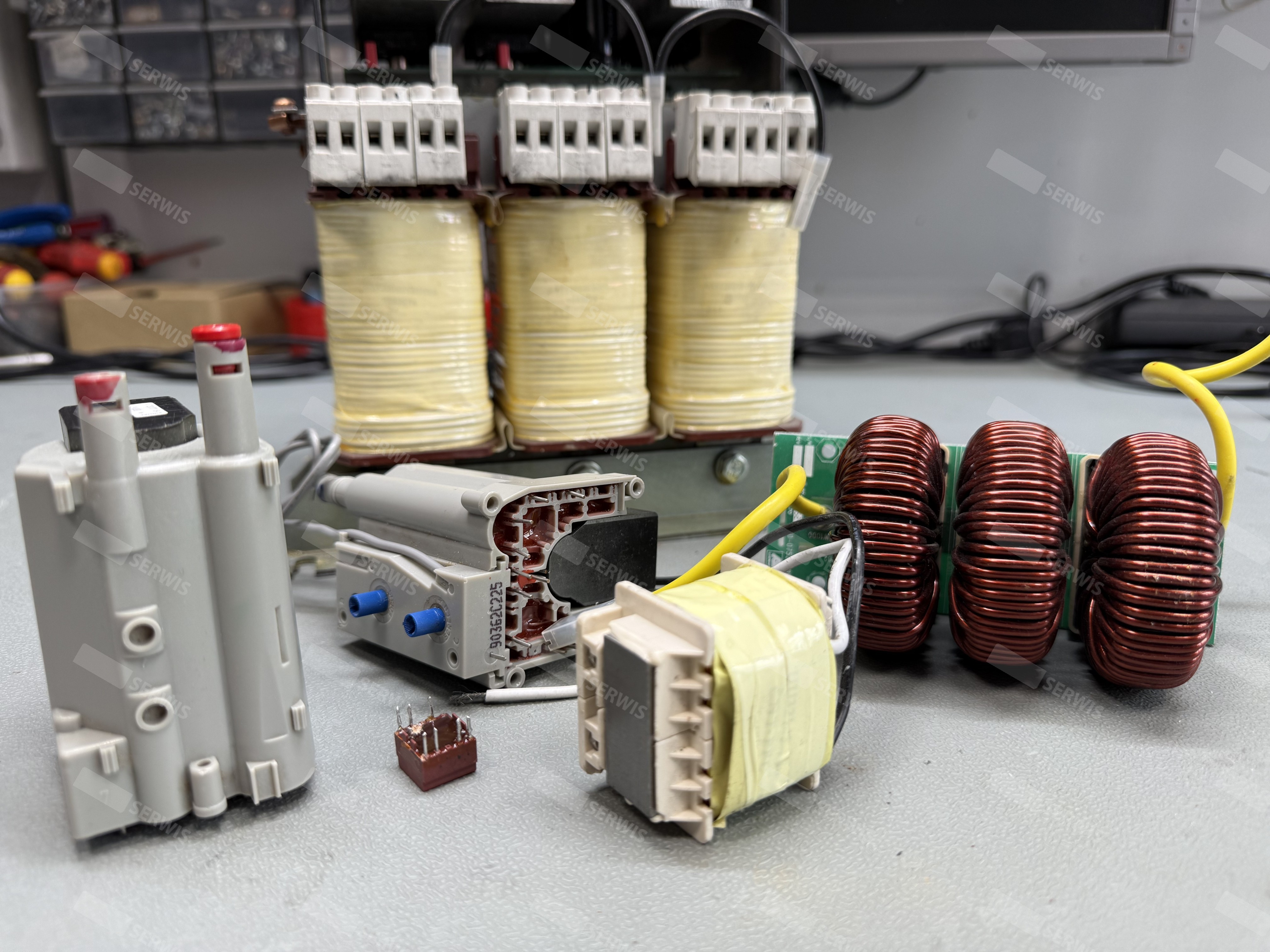
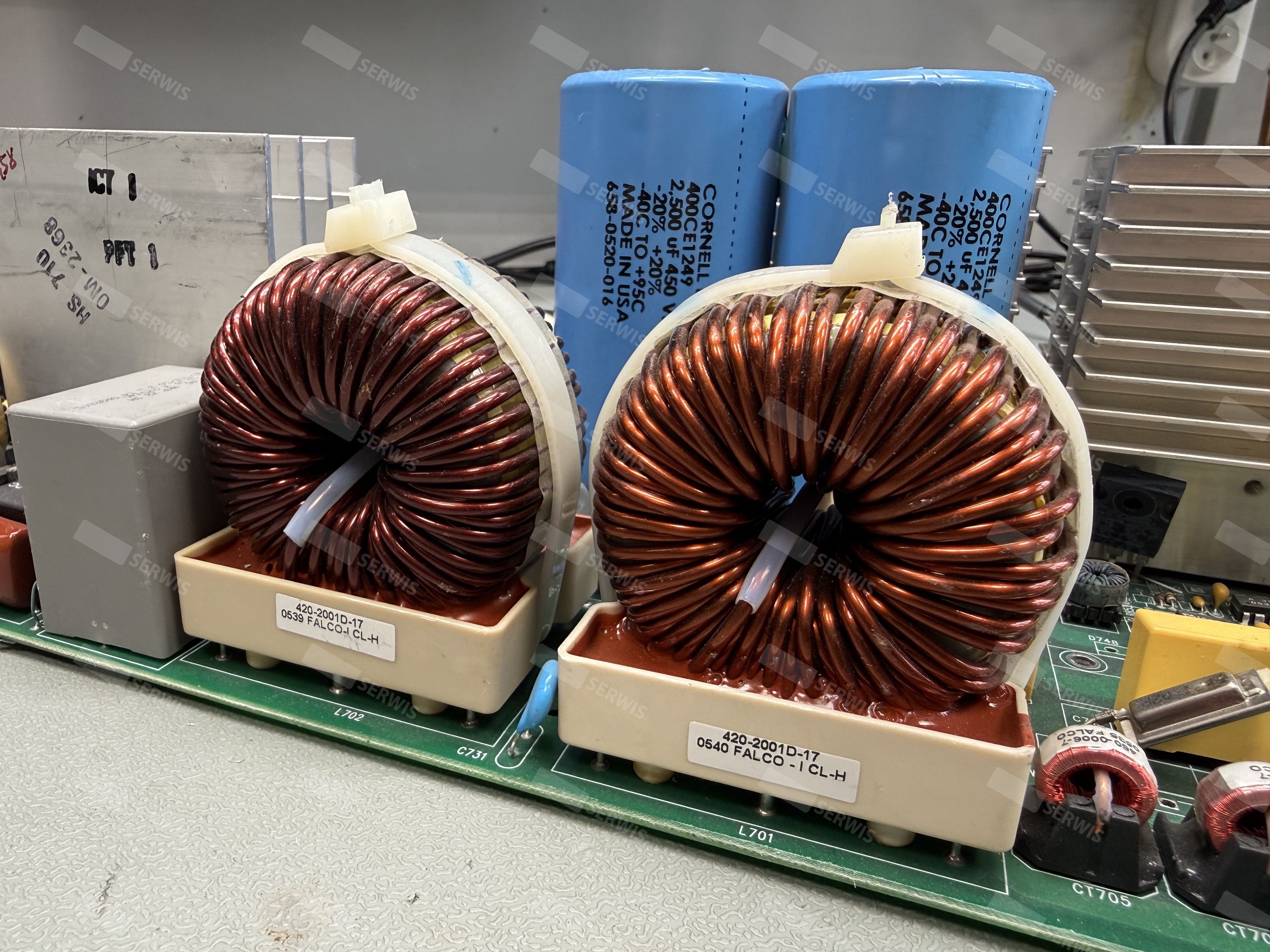
Rewinding of Inductive Components
A common cause of failure is damage to coils, chokes, and transformers. In many service centers, repair stops at this point due to a lack of available spare parts.
We carry out repairs by rewinding and rebuilding these components, restoring their operating parameters and the device's functionality.
All repairs are carried out in-house by experienced specialists with many years of practice in industrial electronics. We employ highly skilled technicians for whom electronics is not just a profession, but a passion.
Our team members hold international IPC certifications in SMD, BGA, µBGA, CSP, and FLIP CHIP technologies, confirming their expertise in modern assembly and repair standards for advanced electronics. Our staff also hold SEP qualifications for the operation and supervision of electrical equipment.
The combination of technological competence and formal electrical qualifications is especially important for industrial equipment, where control electronics work alongside high-power systems.
Since 1996, we have continuously expanded our technical facilities to keep pace with the growing integration level and complexity of industrial electronics.
Our extensive company structure — spanning consumer, industrial, medical, and military electronics divisions, including our Dęblin facility involved in the design, production, and maintenance of flight simulators in cooperation with Military Aviation Works — translates into real, tangible team expertise.
As a result, we perform repairs at the component and structural level, even in cases where standard service providers are limited to module replacement.
Technical Facility Gallery
Technologies and Equipment at Our Service Center
See the diagnostic stations, measurement equipment, and solutions we use in industrial electronics repair.