A&D Lab · Scientific Cooperation
Thermographic Diagnostics of Electronic Components
Applying thermal imaging to non-contact diagnostics of electronic equipment — development of a procedure for use in service conditions.

Dr. Eng. Przemysław Matkowski — Wrocław University of Science and Technology, W-12/Z-5
Project conducted from April 1, 2013 to September 30, 2013, in cooperation with A&D Serwis.
Objectives and Project Assumptions
- A diagnostic procedure that is simple and quick enough to be carried out in a service environment.
- Safe for both the operator and the equipment under test (non-contact measurement).
- Operator equipped with a checklist and a reference thermogram.
- Minimized costs — both for purchasing and for ongoing use of the equipment.
Test Setup and Measurement Parameters
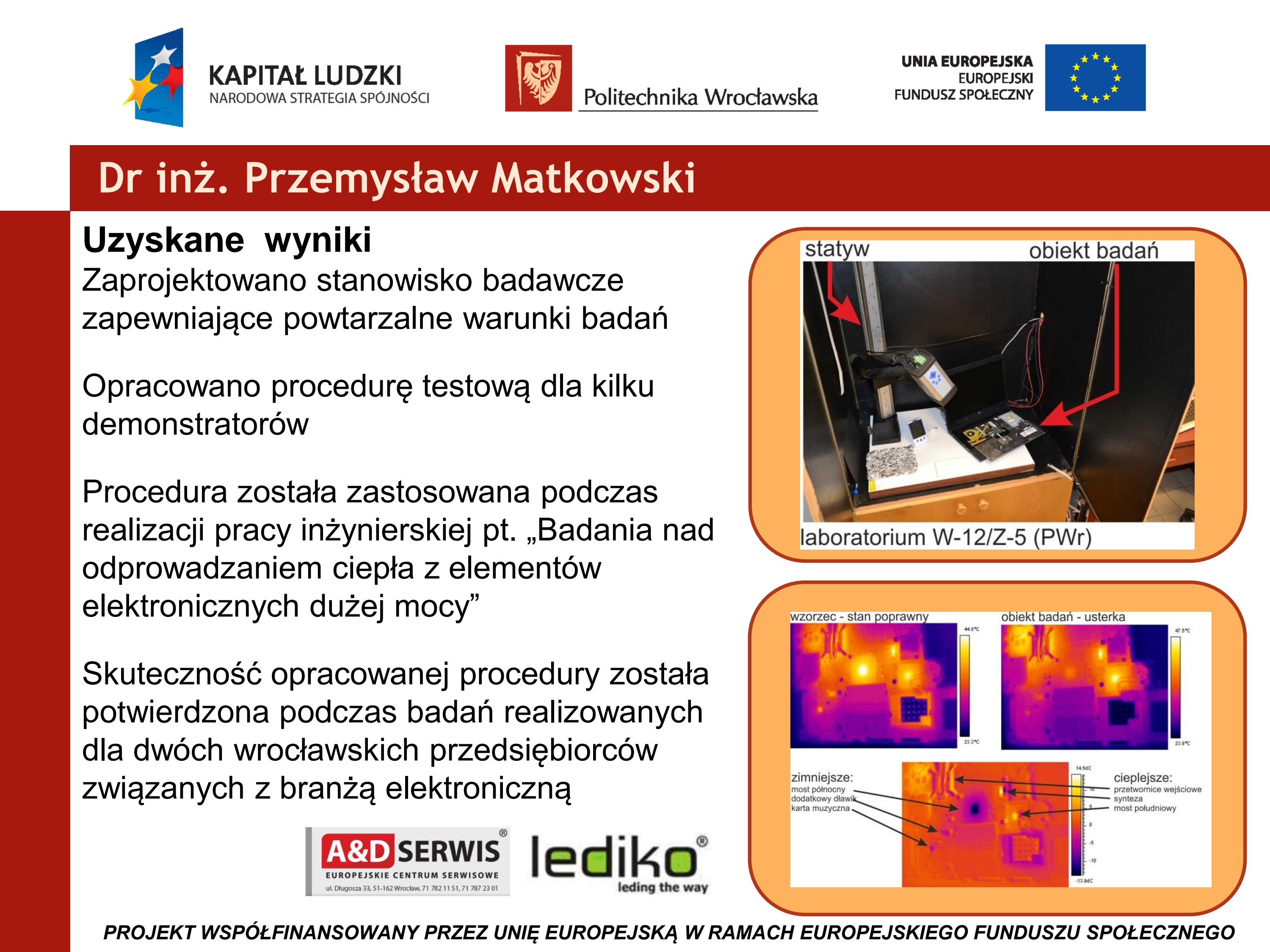
A test setup was designed to ensure repeatable testing conditions. Reliable measurement depends on key factors such as surface emissivity, reflected temperature, humidity, ambient temperature, and camera-to-object distance.
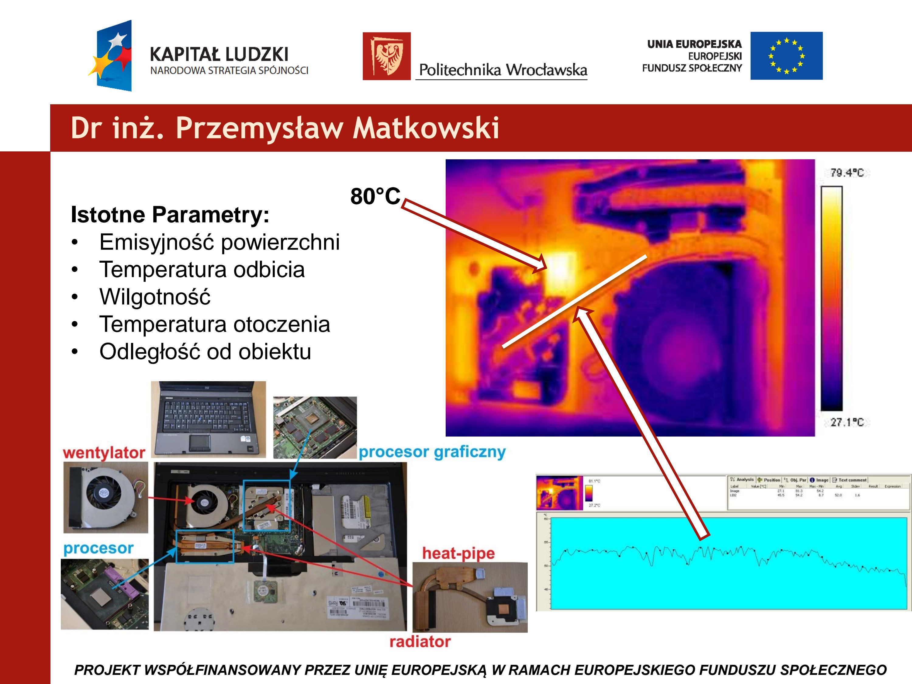
Board Thermal Map — Functional Blocks
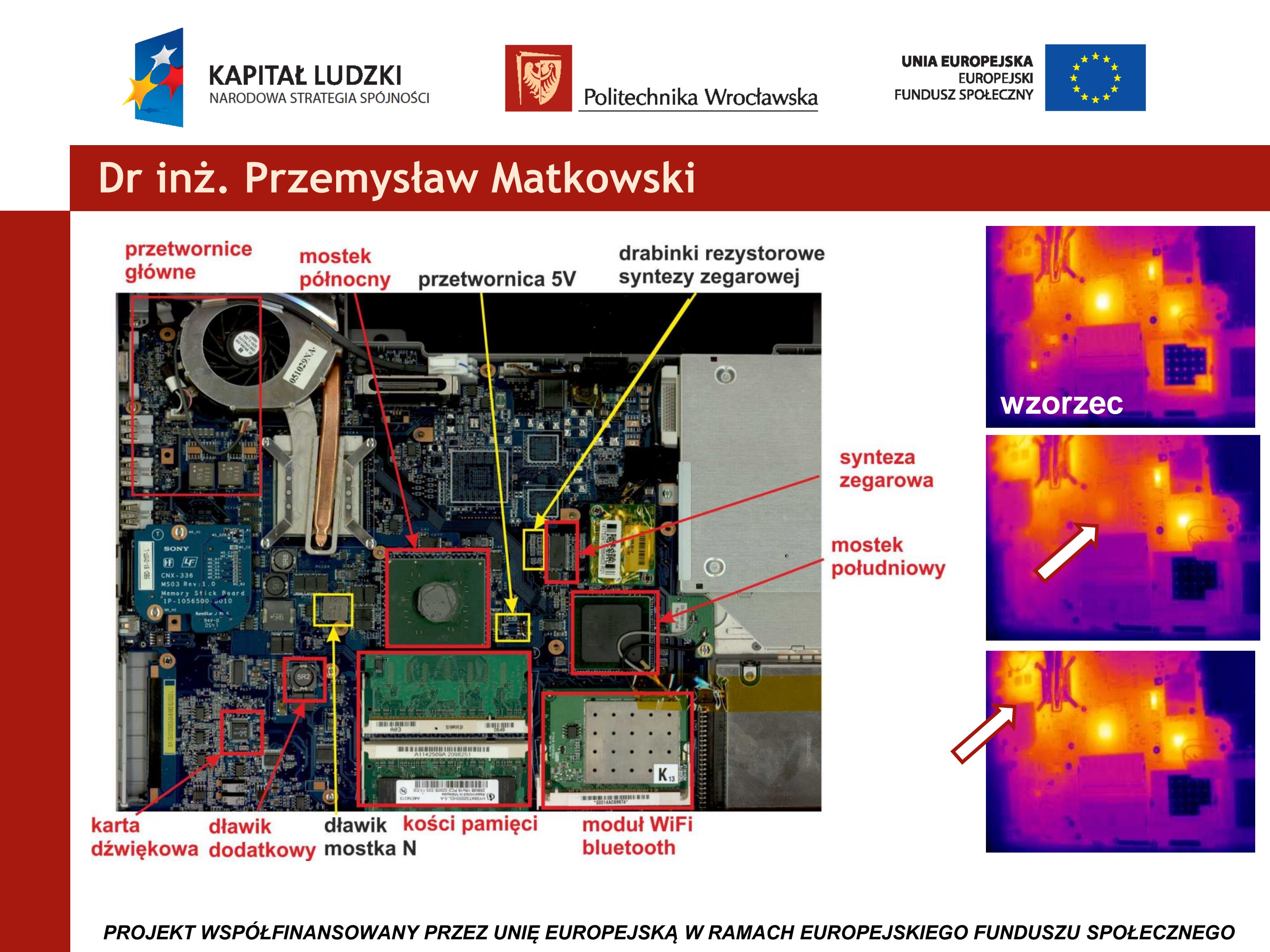
The procedure involves identifying the functional blocks of the motherboard (main converters, N/S bridge, clock generation, chokes, sound card, memory modules, WiFi/Bluetooth) and comparing their thermal signature against a reference thermogram.
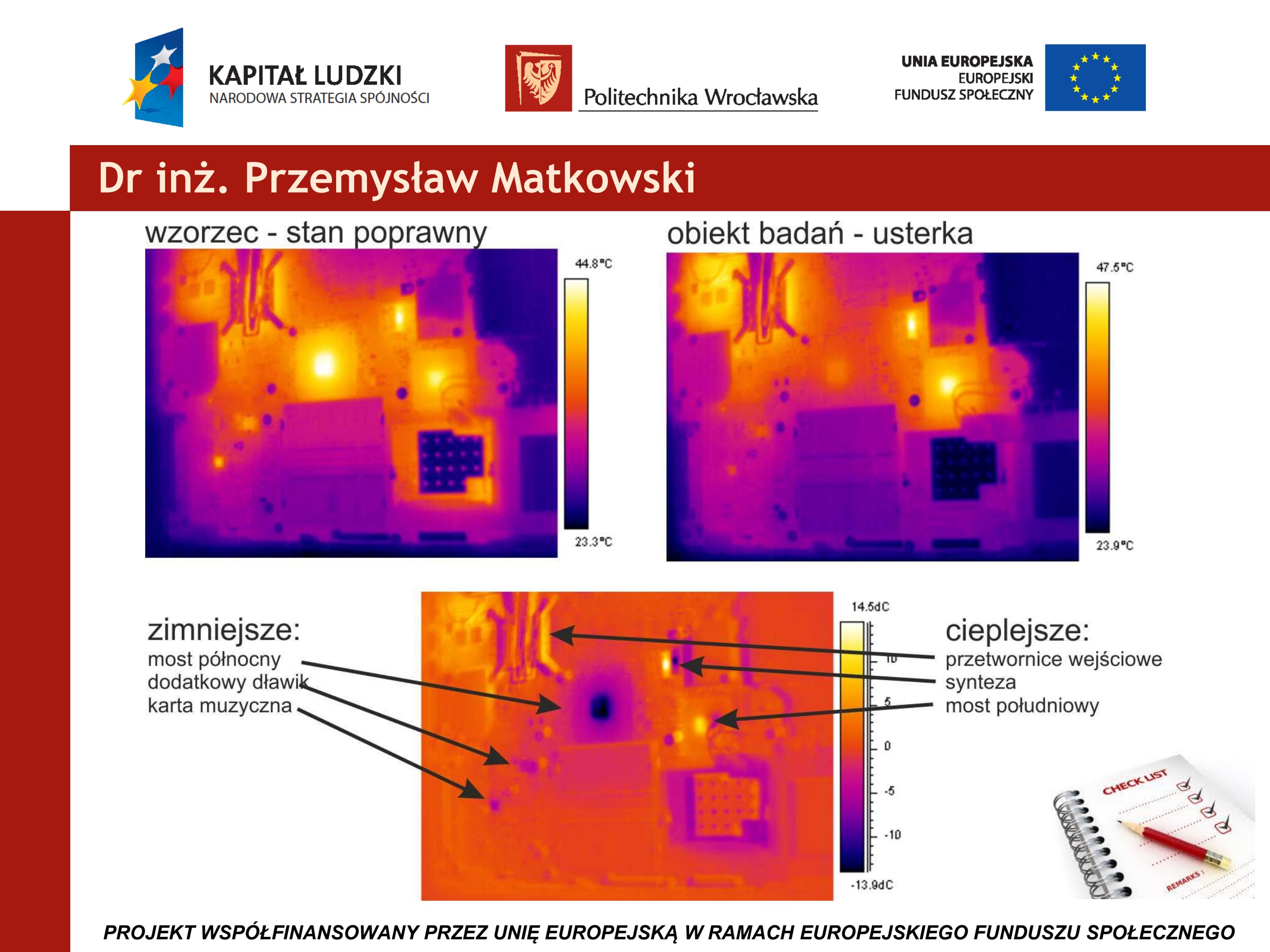
Result 1 — Reference vs. Faulty Unit Comparison
The key methodological finding: a differential temperature map (reference minus test object) clearly identifies the faulty functional blocks. In the case examined, the faults were:
Colder than reference
- north bridge
- additional choke
- sound card
Warmer than reference
- input converters
- clock generation
- south bridge
Result 2 — Current Flow Inside a BGA Package
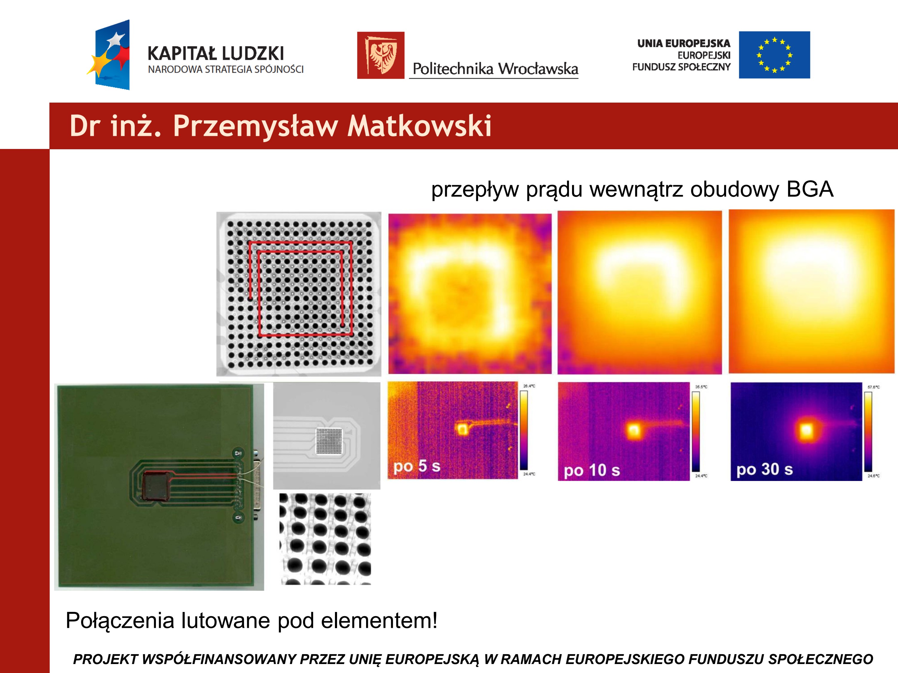
Thermal imaging made it possible to visualize current flow inside a BGA package and identify individual soldered connections beneath the component (BGA balls) without disassembly. Across a 5 s, 10 s, and 30 s sequence, the local temperature rise reached 57.6 °C.
Result 3 — Cracked Solder Joint
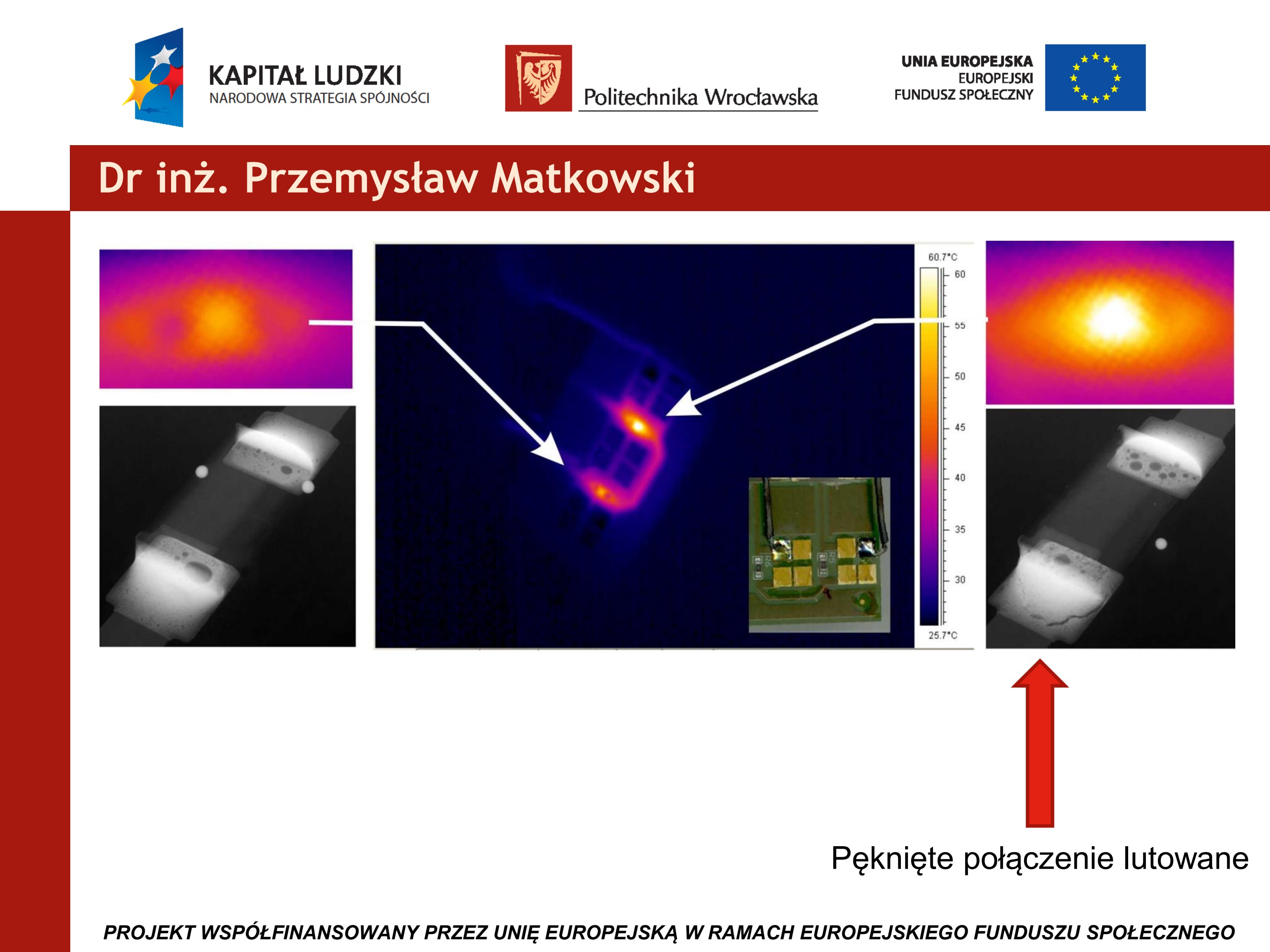
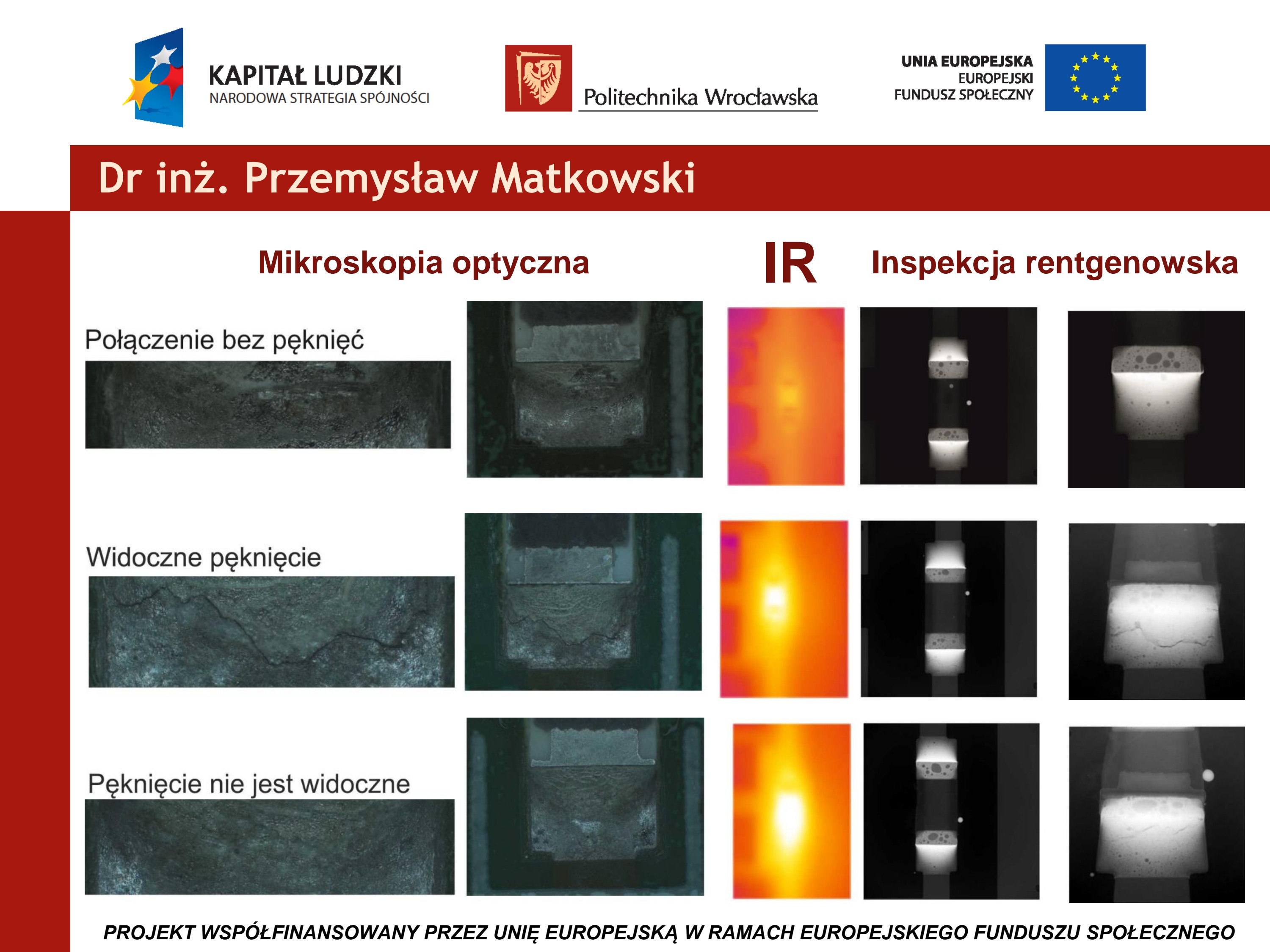
A cracked solder joint produces a characteristic local hot spot reaching up to 60.7 °C. This defect, which is not visible under optical microscopy or in conventional X-ray inspection, is unambiguous in thermal imaging.
Result 4 — Voids Impairing Heat Dissipation (LED)
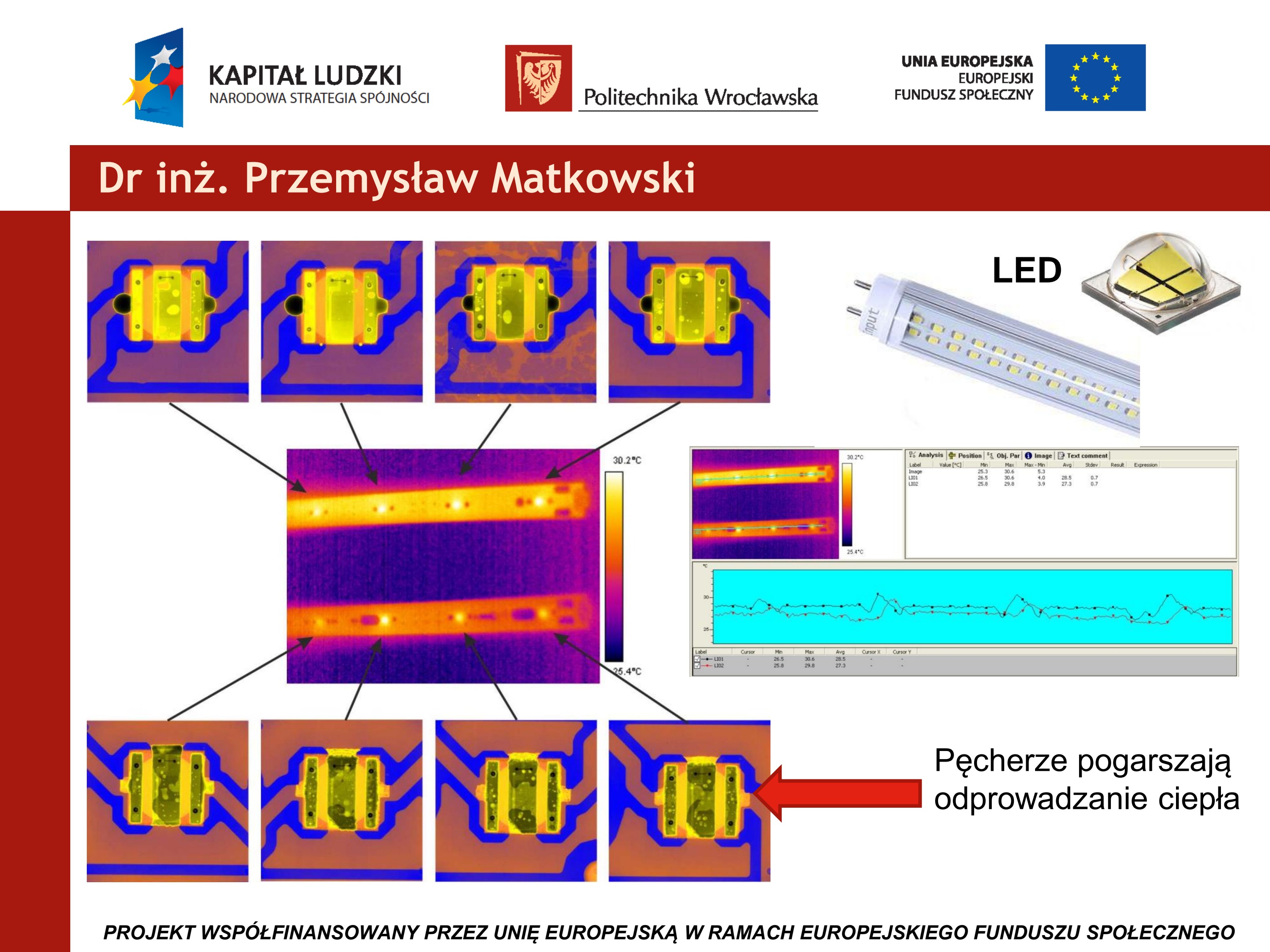
For a high-power LED, a temperature difference was measured between an area with voids in the heat-dissipating layer (L101: max 30.6 °C) and a defect-free area (L102: max 29.8 °C). The procedure detects assembly defects that directly affect component lifespan.
Results and Implementation
- A test setup was designed to ensure repeatable measurement conditions.
- A test procedure was developed for several demonstrator units.
- The procedure was applied in the engineering thesis "Research on Heat Dissipation from High-Power Electronic Components."
- The procedure's effectiveness was confirmed in studies carried out for two Wrocław-based electronics companies, including A&D Serwis.